Premium

A fast solution for the optimal location of the DC combiner box in a PV array

Facebook
Twitter
LinkedIn
Reddit
Email

By Jian Chen, Jiangsu Sainty Machinery Import & Export Corp., Ltd.; JianGuo Chen, PV Engineer, Jiangsu Sainty Machinery Import & Export Corp., Ltd.; XiChen Wang, Jiangsu Sainty Machinery Import & Export Corp., Ltd.

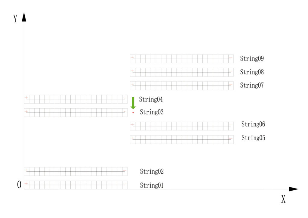
In PV power systems the choice of an appropriate location for the installation of the PV array box (or DC combiner box) is an important undertaking. It is essential that the box be placed so that the amount of DC cabling is minimized in order to not only save cable costs but also reduce voltage losses. This paper presents a fast solution to this problem, based on a mathematical model for the minisum location of the combiner according to the Manhattan metric between the PV array and the DC combiner box. The target function and its optimal solution (i.e. the most economical amount of cabling) for this particular model were obtained, and the optimality of the solution proved by contradiction. The application of this model is illustrated by means of two typical examples, involving an odd and an even number of strings in a PV array. The proposed model is efficient and easy to apply, and as such should be of interest to PV engineers and designers.

Published In

Premium
The period of ‘profitless prosperity’ in the PV industry is finally at an end. Throughout 2013, despite continued economic woes, the PV industry has continued to expand and finally become a global industry. Market forecasts indicating that the sector could reach its next 100GW milestone in just the next two years suggest the industry is on the cusp of another period of strong growth. All the signs confirm this is the case, with utilization rates at their highest level since 2010, companies reporting full order books well into next year and the first tentative announcements of factory capacity expansions making the headlines.
Premium
The second edition of Photovoltaics International was published in November 2008. It includes the cost benefits of conversion of used 200mm semiconductor fabs for the PV industry by CH2M Hill in Fab & Facilities, in-line plasma-chemical etching from Fraunhofer IWS in Cell Processing and NREL presents design criteria for back- and front-sheet materials in PV Modules.

Read Next

Subscribe to Newsletter

Upcoming Events

Solar Media Events
May 1, 2024
Dallas, Texas
Solar Media Events
May 21, 2024
Sydney, Australia