AIKO’s proprietary “self-masked two-step process”, combined with laser patterning, has redefined the way N-Type All Back Contact (ABC) solar cells are made—setting new benchmarks for efficiency, reliability and large-scale production and making Back Contact (BC) technology truly scalable for mainstream adoption.
BC solar cells have long been seen as the most promising pathway to higher efficiency in crystalline silicon photovoltaics. With no front-side grid lines and 100% light absorption, they offer the highest theoretical efficiency. However, for decades, the industry has struggled to scale BC due to its complex manufacturing process and high cost.
AIKO has changed that by introducing a new process that addresses the fundamental challenges holding BC back from mass adoption.
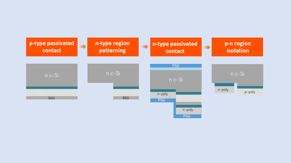
Conventional BC production typically uses a one-step process that forms tunneling oxide and polycrystalline silicon layers—the key charge-selective layers—at the same time. This oversimplified method forces trade-offs, as the ideal process conditions for one region negatively impact the other, resulting in suboptimal passivated contacts and limited efficiency.
AIKO’s breakthrough comes from completely decoupling the formation of the p-type and n-type tunneling oxide and polycrystalline silicon layers. This allows each side of the solar cell to be optimized independently, maximizing the passivation quality and pushing conversion efficiency to new heights.
To further enhance the process, AIKO has pioneered the use of BSG (boron silicate glass) and PSG (phosphorous silicate glass)—materials formed during high-temperature diffusion—as natural, self-aligned masks. This innovation:
- Eliminates the need for external masking and cleaning, reducing contamination risk
- Simplifies the overall process, making it as efficient as traditional one-step methods
- Reduces material consumption, while improving yield and production consistency
This has enabled the production of low-stress, high-uniformity films with exceptional passivation quality, laying the physical foundation formass production of ABC cells with conversion efficiencies exceeding 27%.
To achieve this, AIKO has leveraged its strong R&D capabilities to reconstruct the high-temperature thermodynamic environment through thermal field simulation, finding the optimal balance between laminar flow control and passivation kinetics. The company also developed an intelligent stress-balancing system and applied advanced modeling tools to achieve ultra-precise temperature control within ±0.5°C inside the reaction chamber. These breakthrough process innovations ensure the consistent formation of high-quality tunneling oxide and polycrystalline silicon layers for both the p-type and n-type regions, paving the way for industry-leading cell efficiency and manufacturing stability.
Together, these advancements enable AIKO to produce ABC modules at gigawatt scale with excellent performance, reliability and cost-effectiveness, rapidly approaching the cost levels of mainstream TOPCon and PERC products.
The commercialization of the company’s proprietary self-masked two-step process marks more than just a manufacturing upgrade—it signals a turning point in the solar industry. With ABC technology now mature, scalable and ready for global deployment, AIKO is helping pave the way toward a more powerful and sustainable energy future.