Materials

Premium
Photovoltaics International Papers, Materials
Our EpiNex™ wafers enable higher efficiencies, lower costs and reduced carbon emissions in wafer manufacturing by more than 70% when compared with the conventional Czochralski process in regions that rely on coal-based electricity. NexWafe’s innovative and unique technology creates the opportunity to profitably manufacture ultra-low-carbon green solar wafers.
Premium
Materials, Photovoltaics International Papers
The PV industry is undergoing rapid technology changes that have been driven by the well-documented swift adoption of monocrystalline wafers. Less well understood, however, is that within this wafer technology transition comes a shift to larger wafer sizes, and this includes p-type and n-type mono-Si wafers.
Premium
Materials, Photovoltaics International Papers
The silicon PV industry has predominantly used silicon wafers sliced by a steel wire, with silicon carbide particles (slurry wire – SW) as an abrasive and polyethylene glycol as a coolant. Low yield, high total thickness variation (TTV), significant material waste and short wire lifetime (and thus high downtime) of SW cutting technology have prompted the wafer slicing industry to develop an alternative technology. Researchers have developed diamond wire (DW) cutting technology for slicing the silicon and demonstrated that it overcomes the drawbacks of SW cutting technology. Although the DW cutting technology has been demonstrated for slicing wafers, the wafer surface is different after the conventional acidic texturing in a silicon solar cell process. It is therefore important to improve the existing process or to develop a new process, in order to produce a homogeneous texturization on DW-cut wafers. In this work, a systematic approach has been pursued to improve the existing process by using an additional etchant (a texture additive) in the acidic mixture. Different etch depths and the corresponding mean reflectance were studied. Optical and morphological studies on DW-cut wafers processed with and without a texture additive have been carried out and interpreted in terms of electrical performance.
Premium
Materials, Photovoltaics International Papers
The application of electrically conductive adhesives (ECAs) is a promising alternative to the soldering process for cell interconnection in today’s solar module production. ECAs provide an environmentally friendly solution and offer several other advantages over the conventional solder interconnection technology, such as lower processing temperature, higher mechanical flexibility and replacement of toxic lead. When it is proposed to switch from soldering to adhesive technology in a critical process such as the production of solar cell strings, it is necessary to perform a thorough preliminary analysis of the properties of the materials involved, the material compatibilities and the long-term stability of the interconnections within the PV modules.
Premium
Materials, Photovoltaics International Papers
As the PV industry strives to reach terawatt scale, addressing the last remaining cost centres of the crystalline silicon value chain will play a critical role in ensuring that the industry can continue to achieve lower systems costs, and provide the extremely low levelized cost of electricity (LCOE) required to drive the adoption of this form of energy. Wafer manufacturing remains the single largest cost driver in industrial cell production. While incremental improvements, such as diamond wire (DW) sawing, have helped to lower silicon consumption, wafer manufacturing has lacked the significant step change necessary for achieving dramatic cost reduction.
Premium
Materials, Photovoltaics International Papers
Major progress has been made in the PV industry in the last five years as a result of the extensive use of diamond wire during silicon wafering operations. Productivity has increased and costs have fallen to the point where the price of a monocrystalline wafer cut with diamond wire is approaching the price of a multicrystalline wafer cut using slurry.
Premium
Materials, Photovoltaics International Papers
By the end of 2017 it is expected that boron-doped multicrystalline silicon (p-type mc-Si) wafers will have been used in more than 60% of the world’s manufactured solar cells.
Premium
Materials, Photovoltaics International Papers
The drive towards better Si utilization (g/Wp) has been an obsession in the Si PV industry over the last few decades as one of the key aspects in making photovoltaic energy production competitive. With the cost of Si still making up a third of the final Si solar module cost, there is continued interest in reducing the cost of Si by producing thinner wafers and reducing kerf losses.
Premium
Materials, Photovoltaics International Papers
In the Chinese PV market, multi crystalline silicon firmly holds a large market share compared with monocrystalline silicon, entirely as a result of the development of the Chinese PV industry.
Premium
Materials, Photovoltaics International Papers
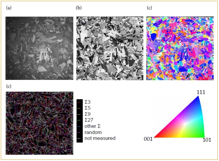
High-performance multicrystalline (HPM) silicon, achieved by nucleation on special seed layers at the crucible bottom, is now increasingly replacing conventional multicrystalline (mc) silicon, which is solidified on the standard silicon nitride coating. The HPM material is characterized by a very fine initial grain structure consisting of small, regularly shaped grains surrounded by a large number of random-angle grain boundaries. These grain structure properties, which differ significantly from those of conventional multicrystalline silicon, lead to a much lower dislocation content in the material, and therefore result in higher efficiencies of the silicon solar cells produced. This paper gives a rough overview of the worldwide R&D activities on HPM silicon in recent years, supplemented by several research results obtained at Fraunhofer IISB/THM. The focus is on the different seeding methods, the grain structure properties and the development of the grain and defect structure over the ingot height, as well as on the main challenges for further improvements in material quality and production costs.

Subscribe to Newsletter

Upcoming Events

Solar Media Events
March 19, 2024
Texas, USA
Solar Media Events
March 26, 2024
Lisbon, Portugal
Solar Media Events
April 10, 2024
Dallas, Texas USA