On June 24th, seven companies, including LONGi, Jinko Solar, JA Solar, and Canadian Solar jointly released the M10 (182mm) monocrystalline silicon wafer. Why is this size of wafer being released in the face of 166mm and 210mm alternative specifications? Is this wafer specification a transition product? This article will explain the associated logic.
1. History Review
The trend of larger photovoltaic modules began in the second half of 2018. At that time, monocrystalline modules using 158.75mm silicon wafers and polycrystalline modules with 166mm silicon wafers first appeared, together with silicon wafers with specifications of 157.4mm and 161.7mm, all larger than the mainstream M2-156.75mm wafer. Initially, the emergence of such products was mainly to obtain an advantage on the customer side by increasing power. The change subsequently triggered the industry to think about whether such a size change was really meaningful without improving basic efficiency: it was found that the power increase brought about by the larger wafer could indeed save on the BOS costs of a power plant, and the size increase could reduce the cost of cell and module manufacturing.
Based on the above, LONGi announced to the industry that larger monocrystalline wafers offered more advantages than polycrystalline wafers. Given the compatibility with existing 100GW cell production capacity, M6 wafers of 166mm were duly launched in May 2019. Through promotional activities, the downstream power plant investment and design sector recognized the system side value brought by the increase in wafer size.
In August 2019, Zhonghuan Semiconductor released a 210mm (G12) wafer. The logic was that photovoltaics should eventually converge with the semiconductor industry, using 12-inch monocrystalline silicon wafers. This specification was responded to by cell manufacturers Tongwei Group and Aiko Solar, with new cell capacity planned according to G12 wafer size, but the application of G12 created a problem of excessive current on the module and system side. It was not until the end of February 2020 that Trina launched a module that used 50 G12 cells. After triple cutting, the problem of excessive current was resolved. However, the design of its five-column cells inevitably has an extra ribbon to form a circuit loop.
The emergence of the G12 silicon wafer led module and integrated manufacturing companies to start thinking about the size and specifications for new production capacity. How big should silicon wafers be after the leap beyond the current parameters? At the beginning of 2020, there were rumors of a size of about 180mm, until on June 24 the specification finally locked in at 182mm.
2. Logical misunderstanding in determining photovoltaic silicon wafer size based on semiconductor criteria
Analysis of module and cell parameters is very complicated, with some being indistinct. Additionally, it is necessary to establish which parameters can be breached and which cannot. A simple scenario is to refer to the semiconductor industry, because the use and processing of silicon in photovoltaics was first derived from the semiconductor industry.
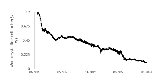
However, this point of view ignores the significant differences between the PV and semiconductor industries. The chip manufacturing process is the core of the semiconductor industry, with the demand for accuracy the reason for the associated high costs. PV cells follow the route of reducing costs, the price per watt recently dropping to around 0.1 dollars. The semiconductor industry can greatly increase the output of chips by increasing their area, thereby reducing costs. At the same time, the increase in size of silicon chips will not affect the shape of a single unit, so there is no need to consider subsequent packaging and applications. The increase in size of photovoltaic wafers and cells will, however, have a significant impact on the packaging and application process. The cost of the cell process is currently only $ 2.8 cents/W, accounting for less than 7% of total system cost. Therefore, having module and system match with cell at all costs is obviously problematic.
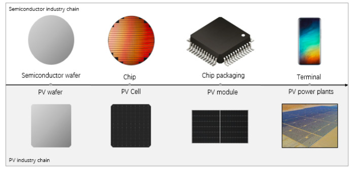
There are other big differences between the two industries. Round wafers are used for the photovoltaic industry and quasi-square wafers are used for semiconductors, with the thickness of a semiconductor wafer 750 μm, whereas the thickness of a photovoltaic wafer has long been reduced to below 200 μm.
In short, the first principle of evaluating photovoltaic products and technology is the LCOE. Without considering differences between power generation capacity and degradation, it can be simplified to the cost of the entire industry chain of products. Any analysis not based on this principle will inevitably lead to an erroneous conclusion.
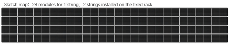
3. The logic of large modules saving BOS costs
In a large-scale photovoltaic system, a certain number of modules will be connected in a series to form a string. Several strings are connected to the combiner box or string-type inverter through a cable. Usually two strings of modules are installed on a single rack and the rack passes through several pile foundations fixed on the ground (the modules on the tracker system can reach 3~4 strings). Increasing the power of a single string can reduce the cost of racks, pile foundations, cables and junction boxes (or string inverters) per watt. In addition, for power plants of the same capacity, the reduction in the number of racks will also reduce the gap area of the rack, thus saving land costs. Therefore, increasing the power of a single string module can save on the overall BOS cost of the power station. Large photovoltaic power plant system voltage from 1000V to 1500V is similar: the increase in voltage leads to an increase in the number of series to increase the power of a single string, thus reducing BOS cost.
In the case of equivalent module efficiency, the use of a large wafer can increase the power of a single string of modules. Because the large wafer increases the current of the module without changing the voltage, the number of modules connected in a series makes the string power increase in the same proportion as the power of a single module. In contrast, when increasing the number of cells to increase module power, the increase in open circuit voltage leads to a reduction in the number of series connections and, with the string power remaining unchanged, the reduction in BOS is limited.
From the perspective of BOS cost, the G12 module takes into account that the conventional design current is too high, and a triple-cut cell is used to reduce the current to only 6.4% higher than an M6 module, the voltage being also 3.8% higher. The BOS cost savings will therefore be very limited.
4. Wafer size determined by module size
For residential rooftop power stations, the area of the M6 60c module has reached 1.8m2, and this size has reached the optimal value from the perspective of single-person installation and flexible roof layout. The size of modules for large-scale power stations can continue to increase. The increase in module size requires consideration on the feasibility of manufacturing and material supply, module reliability and transportation, and system-side compatibility and manual installation.
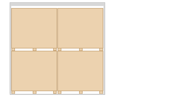
It was found that the short board of the wooden barrel is the problem with the shipping process of the module. The door height of the container (40 HQ) is about 2.57m which limits the width of the module to about 1.13m, providing a margin of nearly 10cm for loading and unloading. The 1.13m width of the module and the number of even-numbered cell columns determine the dimension of the silicon wafer to be about 182mm.
After determining the width of the module, depending on its 72C design, size and weight, other electrical parameters can be deduced to sequentially verify the feasibility of manufacturing and module reliability. The system side compatibility is not a problem. For example, it is very easy for the inverter current to increase from 13A to 15A without changing the existing product architecture, a 15A inverter and a 182mm module matching perfectly. The significant increase in current can bring a significant reduction in BOS cost.
Comparing using a 182mm (M10) wafer module with front power up to 540W with a 500W module using a 210mm (G12) wafer, the advantages are obvious:
• The module power is higher, the space of the container is more fully utilized, and the manual installation cost of the module is lower;
• Module efficiency is higher, and the G12 module cell with 3 cuts and separate long solder ribbon will cause loss of efficiency;
• BOS cost is lower. The current and power of the M10 module are higher than that of the G12 module. Therefore, the string power is higher. The advantage on the system side is very obvious. According to calculations: an M10 module can save at least $0.35 cents/W of BOS cost when using a fixed rack compared to a G12 module, and at least $0.7 cents/W of BOS cost when using a tracker;
• Product manufacturing costs are lower, cell efficiency and yield of the M10 higher, whereas the G12 still has a big problem; on the one hand, the design of M10 on the module side is simple: on the other, the power is higher, and the cost of the module is significantly lower.
As to whether a 182mm module should use 78 cells, as introduced in Chapter 3, increasing the number of cells to increase module power at the system side has limitations. Due to the voltage increase, the string power is unchanged, but the module becomes larger, which brings difficulties and cost increases in product manufacturing, hot spots, mechanical loading test, etc., so the development of a 78C module is of little significance. The idea that the higher the power, the better, is not the case.
In summary
As analyzed above, PV wafer size should be based on LCOE, in terms of system value. This article proposes that single-string power is the key factor in determining the cost of BOS, which is also the reason behind the choice of making the wafer larger rather than increasing the number of cells; comprehensive consideration of various parameters can determine the optimal module size and then the introduction of the 182mm wafer size can follow.
Hence one can answer the questions raised at the beginning of this article: is the M10 182mm wafer the optimal product specification for launching new production capacity when considering the value of the entire industry chain? It is not a transitional product and will end the wafer size dispute. This is sufficient reason for choosing the 182mm wafer for new production capacity.