Authors
Louis Huber, independent consultant at GreenSquare SPRL coordinator of EPKI – European Perovskite Initiative; Dr. Alessandra Alberti and Dr. Ioannis Deretzis from CNR-IMM Institute for Microelectronics and Microsystems Catania Italy and Prof. Dr. Mohammad Nazeeruddin, of EPFL Sion, and founder of Valais Perovskite Solar SA.
Abstract
Organic/inorganic lead halide perovskite solar cells (PSCs) have received global attention because of their excellent photovoltaic performance and ease of fabrication. PSC’s have reached over 24% power conversion efficiency demonstrating that the lead halide perovskites are the most promising class of materials for next-generation thin-film photovoltaics. The unprecedented increase in the device performance from 3.8% to 24% in less than 10 years is mostly due to compositional engineering of mixed cations, and anions, as well as improved processing protocols has made PSC the fastest development of a new material in the PV field.
Though the efficiencies on Lab scale are staggering, the full potential of this burgeoning technology cannot be realized without addressing the following challenges: fighting the degradation of the material is the highest focus for the moment and has several fronts for improvements including within larger scale cells or modules. The other main challenge of the new class of material is the toxicity risks due to the presence of lead. The research community is actively working on the mitigation and reduction of the associated risks. The exceptional properties of this material combined alongside its inherent relative lower costs have already triggered the interests of industries and start-up worldwide while on a European regional level, EPKI for European Perovskite Initiative was formed gathering all the significant players in the field.
Introduction
Calcium titanate Perovskite (ABX3) is a class of semiconductors discovered in the middle of the 19th century and named after Russian mineralogist Lev Perovski.[1] This ABX3 crystal structure was first studied as a PV absorber material in 2009 by Tsutomu Miyasaka et al., by mixing lead bromide and methylammonium bromide and obtaining an instant crystallization through a spin coating process. This first PSC generated a 3.8 % Power Conversion Efficiency (PCE), and was based on a mesoporous TiO2 anode.[2] At that time, the device would not last more than a few seconds since the electrolyte dissolved the perovskite crystals quasi instantly. Later helped by Oxford University, the recipe was tuned with the addition of an organic hole conductor material into the device that conferred enhanced stability and efficiencies at around 10%.[3] Later came the discovery that perovskite is not only a light absorber but also as an electron and hole conductor itself changing the vision of the research community. [4]
PSC typically consists of a conducting glass (or polymer) deposition, an electron extraction layer typically TiO2 or SnO2, then comes the essential active-perovskite material and on top a hole transporting material and electrodes usually gold, terminate the stack (The inverted configuration being also an option). [5, 6] One of the core quality of the Perovskite is the tuneability of its bandgap from 1.15 to 3.06 eV depending on the interchange and mix of different “A” cations such as rubidium (Rb) cesium (Cs), methylammonium (MA) or formamidinium (FA) as well as the associated metals “M” or halides “X”: The tuning options are endless. Large bandgaps perovskite materials are used for non-PV applications such as photodetectors, LED, sensing and X-ray detection, when photovoltaic requires a typical 1,2 to 1,4 eV. [7]
PSC’s are being developed as both single junction, and multiple layers of perovskite (multiple junctions) [8] as well as transparent solar cells and the promising tandem configuration such as c-Si/ perovskite and CIGS/perovskite.[9] At a later stage, the potential of concentrated perovskite could be a path towards higher efficiencies.
The interest of the research community literally skyrocketed in the past 10 years and laboratories worldwide were racing for the highest conversion efficiency which in early 2019 reached an astonishing 24.2% in a single-junction architecture. Further, the combination of semi-transparent / Perovskite layers on top of other PV materials, already resulted in a 28% c-Si/Pk, a 25.6% CIGS/Pk and a 25% Pk/Pk tandem efficiency, all above record cell efficiencies of the bottom PV cell. [10]
Scaling-up to larger areas
Whilst laboratory scale PSC’s are the size of a coin and are breaking efficiencies records, one of the challenges remains in up-scaling to larger areas. Device architecture as well as the choice of the sandwiching contacting materials (hole transport layer and electron transport layer – ETL and HTL respectively) play a major role for upscaling to modules and panels. Highly efficient Perovskite Solar Modules (PSMs) or mini-modules in the direct n-i-p structure are reported in the literature with a PCE of 16% on 10cm2 and 12.6% on 50cm2. Besides the intrinsic losses due to size effects, it must be clear that the process transfer from single solar cells to large area arrays of devices is not trivial and since it is about controlling the nucleation and growth of perovskite grains/crystals uniformly on a large area. Important to mention here that most of the record devices were made with solvent quenching which is not scalable. Intrinsically low cost, versatile chemical methods for industrial scale production which fully avoid solvent residues and collateral effects are yet to be developed. In parallel to chemical methods, physical approaches are being explored, since they would intrinsically guarantee low-contaminant level, almost zero waste and high production throughput for reproducible and reliable processes. In addition, physical processing steps would be more likely integrated in established flow-charts for production of inorganic solar cells or in view of possible business conversion of existing semiconductor industries to perovskite solar cell manufacturing.
In this aspect, automatic processes combining superior material deposition control and high throughput are to be successfully applied for getting the expected low cost PSMs. Therefore, significant efforts have been spent to boost up large-area methodologies such as: ink-jet, screen-printing, spray-pyrolysis and doctor-blade coating or roll to roll printing in combination with ultrasonic spray coating or vapor deposition. It is fair to admit that many of these deposition methods have already been developed and tested more generally for thin film PV.
It is however acknowledged largely that Perovskite-based PV is very promising in terms of cost efficiency: The advantages of perovskites PV with respect to silicon PV stands on their easy and low cost synthesis, cheap precursors, low-temperature solution processing and possibly high throughput manufacturing and the cells are also displaying rather high efficiencies, great low light performance, as well as low weight (ideal on foils). This theoretical cost advantage is essential for its future success but equally important will be the long term stability of its performance to guaranty the best LCoE.
Current levers for improving stability
As mentioned above, the Perovskite material is largely tunable and the choices over its composition of the cations mix, its surface morphology and crystal growth and orientation have been a major focus over the past decade. Different compositions of the material influence many factors such as ion migration, charge carrier diffusion and recombination, defect density, hysteresis behaviors, FF (fill factor), Voc (open circuit Voltage. These all influence the efficiency and stability and require thorough compositional engineering of materials.
As a main concern, hybrid perovskites degrade into their precursor materials when humidity, temperature and light act on their perovskite structure. Humidity tends to penetrate into the lattice either forming new water-based structures or directly reacting with the organic cations. Light acts as a catalyst for the interaction between environmental oxygen and the perovskite, while relatively high temperatures (above 50-60 ° C for CH3NH3PbI3) give rise to a slow material degradation through the evaporation of volatile organic species. In all cases, the perovskite transforms into a yellowish inorganic material lead iodide, which is photo-inactive. Moreover, the softness of the inorganic lattice is prone to the migration of ions that can move under the influence of an external electric field. Finally, the interfaces of the perovskite with its neighboring materials can be centers of carrier recombination, i.e., areas where electrons and holes recombine prior to their capture by the electrodes. Strategies like the encapsulation of the solar cells and the creation of a protecting environment can mitigate most issues related to the impact of water or oxygen. The engineering of more robust perovskite interfaces involving two-dimensional perovskites will help to reduce carrier recombination, while the mixing of organic and inorganic cations (e.g. formamidinium, methylammonium, cesium, rubidium, iodine and bromide) will greatly improve the intrinsic robustness of the perovskite lattice while maintaining solar cell efficiencies high. Last but not least, great efforts have to be put on improving solar cell device architectures.[11]
Perovskite integration into the device architecture raises some specifics on the coupling between materials of differing natures. The device architecture has been conveniently moving form n-i-p to p-i-n structure, that does not simply imply an inversion of the sequence of the electron (n) vs. the hole transporting layer (p). The choice is mainly pushed by the need of avoiding the commercial spiro-OMeTAD as hole transporting material (p-type) that not only increases the cost of production but primarily can introduce deterioration of the interface with the perovskite layer under operating conditions.[12] Alternative HTL materials are under the spotlight including organic, [13] inorganic [14] and carbon-based [15] layers. In addition, p-i-n architectures are more suitable to be combined in tandem with Silicon-solar cells currently perovskite and silicon solar cells have been demonstrated to work in tandem, both in 2-terminals 82T) or 4-terminals (4T) stacked configuration [16]. Oxford-PV in the UK in collaboration with the Fraunhofer Institute in Germany recently (01-2019) claimed an overall efficiency as high as 28% over 1cm2 Si-Perovskite tandem solar cells, certified by NREL [17]; concomitantly in the literature, an efficiency of 25.2% is reported by Sahli et al., for two terminal multiple-cations-anions lead-perovskite and c-Si heterojunction solar cells. Monolithic tandem Silicon-Perovskite cells are expected to even get up to 46% theoretical efficiency using a tailored top perovskite solar cell at Eg~1.75 eV [17b].
Heterogeneous material’s coupling with perovskite in a sandwiched stacking can introduce non-radiative recombination pathways or charge trapping with impact on Voc (open circuit Voltage) and Jsc (short current density)[18] further enhanced during operation under temperature, time and electric field. Interfaces are indeed relevant [1 ] and this opens the field for further development of ETL and HTL materials.
Beyond the design of the perovskite layer and the HTL, considered as pivotal aspects towards industrialization of PSC, other parts of the stack are under scrutiny of the scientific community:
- In the search for low cost back contact electrodes material alternatives to gold are being considered including low cost-metallic conductive layers or even promising polymers-based or even carbon-based materials.
- Investigating new substrates to replace lab standards FTO or ITO which would combine transparency, conductivity low processing temperature and low costs, without lowering the FF values of the entire cells (i.e. carbon graphene, polystyrenes sulfonate). Flexibles substrates also have a promising future.
Environmental challenges for today and tomorrow research: presence of lead and its mitigation.
A number of studies have performed life cycle assessments (LCA) at laboratory or pre-industrial processes and since the expected lifetime are still unknown, it is still difficult to get to some clear conclusions. However, thanks to the usage of abundant synthetic components (avoiding mining or heavy purification process), a very low material usage and a low processing temperature, Perovskite PVs have very strong arguments to become one of the most environmental friendly technology holding very high performances in terms of CO2/kWh g compare with other technologies as well as a very good Energy Payback Time (EPBT) or Energy Return on Investment (ERoI).
In spite of the above arguments, PSC are not free of environmental impacts and most commonly used PSC contains lead for which health and environmental risks are well known. While the substitution or reduction of lead is an active area of research, as of now no suitable alternative has been found. As the lead content in consumer products is limited to 0.1% in any homogeneous layer, PSMs are in conformity with the RoHS directive 5,12 and meanwhile, properly encapsulated modules introduce very low risk of leakage and the usage of self-healing encapsulants and/or other containment concepts will further mitigate potential leakage rate.
The entire Perovskite community is dedicated to work on the reduction of any environmental impacts this new class of material would carry, however today already a detailed study has shown that the avoided impacts on eco-toxicity through the use of PSC were significantly outweighing the additional impacts.
Perovskite business developments: a map of what’s going on around PCS worldwide
EPKI members:
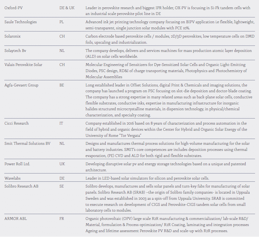
Other examples of Perovskite active companies worldwide: Swift Solar in USA, Tandem PV in USA, Greatcells solar in Australia, Sekisui / Panasonic / Toshiba in Japan, Fujifilm in Japan, Microquanta Semiconductor in CN, Wonder Solar in CN, GCL Nano in CN, Ruitai Material in CN, Xiamen Weihua Solar Co., Ltd. in CN, Front Materials in TW, Frontier Energy Solution KR, Energy Material Corp USA, Heliatek in DE, Hunt Energy Enterprises, Dyenamo, Peccell Technologies Inc In JP, Tosoh Corporation in JP. Lightyear in NL.
Introducing EPKI mission and future challenges for this initiative
European Universities, Research Institutes and industry players involved in the development of perovskite technologies have agreed to the creation of a collaborative platform: the EPKI for European Perovskite Initiative. This group animated by consultant Louis HUBER and Ronn ANDRIESSEN Director at Solliance, is dedicated to gathering all significant parties working in this field with the objectives of raising the awareness on perovskite-based PV at European and on national levels, to facilitate joint-research programs and synergies among universities, institutes and companies. We consider Perovskite to be a great chance for European industry to relaunch production investments and to re-conquer market shares in the worldwide booming PV industry. Betting on new generation PV technology will allow a new type of PV products combining low cost, high level of customization and aesthetics.
The first edition of EPKI whitepaper has been released in September 2019 conveying a common vision of its members, as of today 61 from 18 countries. It is available for download on www. epki.eu
Authors
Louis Huber: Consultant and Business Developer with 12 years’ experience in PV mainly on installation, EPC contracts, PV modules sales and sourcing, European BD and collaborations. He is now working independently from Brussels and Paris within the EPKI program, as promoter and mediator between Research, Industry and political arena.
Alessandra Alberti: Ph.D. cum laude in Physics and Researcher at Institute for Microelectronics and Microsystems of the National Research Council of Italy in Catania from January 2001. Expert in physical deposition methods (sputtering and sublimation) and High-Resolution X-Ray Diffraction/Reflection. Long-lasting collaborations with the prof. T.Miyasaka’s team. Author of >100 JCR papers and Italian/USA patents.
Ioannis Deretzis : Doctor and Researcher at the institute of Microelectronics and Microsystems in Catania, Italy. He is working on various fields of computational materials science and theoretical solid-state physics. His current research interests focus on low-dimensional materials and hybrid perovskites.
Prof. Nazeeruddin: Current research at EPFL focuses on Perovskite Solar Cells and Light-emitting diodes. He has published more than 630 peer-reviewed papers, ten book chapters, and inventor/co-inventor of over 75 patents.He is elected to the European Academy of Sciences (EURASC), and Fellow of The Royal Society of Chemistry.According to ISI listing, he is one of the most cited chemists in 2014, 2015, 2016, 2017 and 2018, and one of the 20 scientists identified by Thomson Reuters as The World Most Influential Scientific Minds.
References
[1] Saparov, B and Mitzi, D, Chemical Reviews, 2016, 116, 4558.
[2]. Kojima, A., Teshima, K., Shirai, Y. & Miyasaka, T. Organometal Halide Perovskites as Visible-Light Sensitizers for Photovoltaic Cells. J. Am. Chem. Soc. 131, 6050–6051 (2009).
[3]. Lee, M. M.; Teuscher, J.; Miyasaka, T.; Murakami, T. N.; Snaith, H. J. Science 2012, 338 (6107), 643.
[4] Gao, P.; Grätzel, M.; Nazeeruddin, M. K. Energy Environ. Sci. 2014, 7, 2448
[5]. Burschka, J.; Pellet, N.; Moon, S.-J.; Humphry- Baker, R.; Gao, P.; Nazeeruddin, M. K.; Grätzel, M. Nature 2013, 499, 316.
[6]. Malinkiewicz, O.; Yella, A.; Lee, Y. H.; Espallargas, G. M. M.; Graetzel, M.; Nazeeruddin, M. K.; Bolink, H. J. Nat. Photonics 2014, 8, 128.
[7]. Yang, Z.; Rajagopal, A.; Jo, S. B.; Chueh, C.-C.; Williams, S.; Huang, C.-C.; Katahara, J. K.; Hillhouse, H. W.; Jen, A. K. Y., Nano Lett. 2016, 16 (12), 7739-7747.
[8]. Rajagopal, A.; Yang, Z.; Jo, S. B.; Braly, I. L.; Liang, P.-W.; Hillhouse, H. W.; Jen, A. K.-Y., Highly Efficient Perovskite–Perovskite Tandem Solar Cells Reaching 80% of the Theoretical Limit in Photovoltage. Adv. Mater. 2017, 29 (34), 1702140.
[9]. Bush, K. A.; Palmstrom, A. F.; Yu, Z. J.; Boccard, M.; Cheacharoen, R.; Mailoa, J. P.; McMeekin, D. P.; Hoye, R. L. Z.; Bailie, C. D.; Leijtens, T.; Peters, I. M.; Minichetti, M. C.; Rolston, N.; Prasanna, R.; Sofia, S.; Harwood, D.; Ma, W.; Moghadam, F.; Snaith, H. J.; Buonassisi, T.; Holman, Z. C.; Bent, S. F.; McGehee, M. D., 23.6%-efficient monolithic perovskite/silicon tandem solar cells with improved stability. Nat. Energy. 2017, 2, 17009.
[10]. https://www.nrel.gov/pv/assets/images/ efficiency-chart-20180716.jpg
[11]. Ajay Kumar Jena, Ashish Kulkarni, and Tsutomu Miyasaka, Halide Perovskite Photovoltaics: Background, Status, and Future Prospects, Chem. Rev. 2019, 119, 3036−3103
[12] Ajay Kumar Jena, Youhei Numata, Masashi Ikegami and Tsutomu Miyasaka, Role of spiro- OMeTAD in performance deterioration of perovskite solar cells at high temperature and reuse of the perovskite films to avoid Pb-waste, J. Mater. Chem. A, 2018, 6, 2219
[13] Maxence Urbani, Gema de la Torre, Mohammad Khaja Nazeeruddin and Toma ́s Torres, Phthalocyanines and porphyrinoid analogues as hole- and electron-transporting materials for perovskite solar cells Chem. Soc. Rev., 2019, 48, 2738
[14] Jiangzhao Chen, Nam-Gyu Park, Inorganic Hole Transporting Materials for Stable and High Efficiency Perovskite Solar Cells, J. Phys. Chem. C20181222514039-14063
[15] Haining Chen and Shihe Yang, Methods and strategies for achieving high- performance carbon-based perovskite solar cells without hole transport materials J. Mater. Chem. A, 2019, 7, 15476
[16] Dong Zhang, Mehrdad Najafi, Valerio Zardetto, Maarten Dörenkämper, Xuedong Zhou, Sjoerd Veenstra, L.J. Geerligs, Tom Aernouts, Ronn Andriessen High efficiency 4-terminal perovskite/c- Si tandem cells, Solar Energy Materials and Solar Cells 2018, 188, 1–5
[17] https://www.oxfordpv.com/news/oxford-pv-sets-world-record-perovskite-solar-cell: last access 31-01-2019
[17B] Giles E. Eperon, Maximilian T. Hoerantner and Henry J. Snaith, Article published in Nature Reviews Chemistry 1, 0095 (2017), doi:10.1038/s41570-017-0095
[18] Martin Stolterfoht, Pietro Caprioglio, Christian M. Wolff, José A. Márquez, Joleik Nordmann, Shanshan Zhang, Daniel Rothhardt, Ulrich Hörmann, Alex Redinger, Lukas Kegelmann, Steve Albrecht, Thomas Kirchartz, Michael Saliba, Thomas Unold, Dieter Neher The perovskite/transport layer interfaces dominate non-radiative recombination in efficient perovskite solar cells arXiv:1810.01333 [physics.app-ph]
[19] Philip Schulz, David Cahen and Antoine Kahn, Halide Perovskites: Is It All about the Interfaces? Chem. Rev. 2019, 119, 3349−3417
[20] A decade of perovskite photovoltaics: This year marks ten years of organic–inorganic perovskite solar cell research. Now, after achieving remarkable gains in performance, applications are starting to make their way out of research laboratories into the real world. Nature Energy, 4,1 (2019)
[21] Rui Wang, Muhammad Mujahid, Yu Duan, Zhao- Kui Wang, Jingjing Xue, and Yang Yang, A Review of Perovskites Solar Cell Stability Adv. Funct. Mater. 2019, 1808843
[22] A. Alberti, I. Deretzis, G. Pellegrino, C. Bongiorno, E. Smecca, G. Mannino, F. Giannazzo, G. G. Condorelli, N. Sakai, T. Miyasaka, C. Spinella and A. La Magna: Similar Structural Dynamics for the Degradation of CH3NH3PbI3 in Air and in Vacuum. ChemPhysChem, 2015, 16, 3064–3071.
[23] Ceratti, D. R., Rakita, Y., Cremonesi, L., Tenne, R., Kalchenko, V., Elbaum, M., Oron, D., Potenza, M. A. C., Hodes, G., Cahen, D. Self-Healing Inside APbBr3 Halide Perovskite Crystals, Adv. Mater., 2018, 30, 1706273
[24] Alessandra Alberti, Ioannis Deretzis, Giovanni Mannino, Emanuele Smecca, Filippo Giannazzo, Andrea Listorti, Silvia Colella, Sofia Masi and Antonino La Magna Nitrogen soaking promotes lattice recovery in polycrystalline hybrid perovskites, Advanced Energy Materials, Adv. Energy Mater. 2019, 9, 1803450.
[25] Alberti A., Bongiorno C., Smecca E., Deretzis I., La Magna A. and Spinella C., Pb clustering and PbI2 nanofragmentation during methylammonium lead iodide perovskite degradation, Nat. Commun., 2019, 10:2196 1-11
[26] Alessandra Alberti, Emanuele Smecca, Salvatore Sanzaro, Giovanni Mannino, Ioannis Deretzis and Antonino La Magna Hybrid perovskites for photovoltaics: Story, challenges and opportunities, Riv. Nuovo Cimento, 2019, 42, 301-366, DOI: 10.1393/ ncr/i2019-10161-5