Fab & Facilities

Premium
Fab & Facilities, Photovoltaics International Papers
Production equipment is the backbone of the PV industry, but the equipment sector is suffering because of overcapacity. The 2012 global capacity utilization is at 55% for crystalline silicon (x-Si) module production, 70% for cadmium telluride (CdTe) and 80% for copper indium gallium (di)selenide (CIGS). Under these market conditions, there are almost no expected capacity expansions in the near term. The overcapacity has driven the average selling price (ASP) for modules significantly lower, resulting in hyper-competition in the PV industry, where almost all PV companies recognize the importance of product differentiation while still reducing costs. These market conditions present an opportunity for equipment manufacturers to differentiate their offerings through enabling lower production costs and higher efficiency of cells and modules.
Premium
Fab & Facilities, Photovoltaics International Papers
The cleaning performance of three different fluorine-containing precursors – sulphur hexafluoride (SF6), nitrogen trifluoride (NF3) and molecular fluorine (F2) – is compared from theoretical, experimental and commercial points of view. Experiments were performed using an Oerlikon Solar KAI Gen 5 (1300mm x 1100mm) R&D platform. For the experiments with F2, an ‘on-site/on-demand’ generator from The Linde Group was installed at the Oerlikon Solar facility in Trübbach, Switzerland. The SF6-based cleaning process was found to be up to 75% less efficient than the corresponding NF3 or F2 process. A comparison between NF3 and F2 indicates that a significantly larger process window is available for reactor cleaning when F2 is used in place of NF3. This leads to both time and gas mass savings, improving productivity and bringing down the cost of ownership of the reactor cleaning process. As a direct consequence, Oerlikon Solar has decided to transfer the process to their production KAI MT plasma-enhanced chemical vapour deposition (PECVD) platforms.
Premium
Fab & Facilities, Photovoltaics International Papers
What does an industry need for sustainable, long-term success? A market, customers and suppliers, and – most certainly – excellent products that can be sold. When looking at various different mature industries there is one thing they all have in common – they have industry-initiated roadmaps! With SEMI’s experience in the semiconductor industry over the last 40 years, the example of the International Technology Roadmap for Semiconductors (ITRS) has proved that pre-competitive industry collaboration among the supply chain and among competitors leads to a reduction in costs, a better time to market and an increased efficiency. Moreover, it helps all players to benefit from jointly solved manufacturing challenges.
Premium
Fab & Facilities, Photovoltaics International Papers
Although the different roadmaps for PV vary somewhat from each other, the bottom line always remains the same: exponential growth is predicted over the next 5 –10 years. The latest cell technologies meet the demand for grid parity even in central Europe and PV will therefore continue to be the most popular source of renewable energy. In consequence, the whole PV industry has developed from a niche product towards mass production. Every player along the entire value chain is now faced with the need to stay profitable while meeting the ever-increasing demands of the market. Implementing suitable automation can improve competitiveness and thus pave the way to becoming or remaining successful in this turbulent market.
Premium
Fab & Facilities, Photovoltaics International Papers
Several PV module producers have performed a carbon footprint analysis and published a sustainability report as part of their corporate social responsibility policy. Comparison of carbon footprint results is difficult because several international standards and life cycle assessment (LCA) databases are used. No product footprint category rules (PFCR) or product category rules (PCRs) for photovoltaics exist, so LCAs are performed with varying underlying assumptions. Furthermore, a fair comparison can only be made when all environmental footprints of a product are taken into account.
Premium
Fab & Facilities, Photovoltaics International Papers
As a relative newcomer to the industrial world compared to more mature manufacturing sectors, the PV industry has not yet been subject to consistent environmental regulatory standards internationally. Like all industries that have preceded it, PV manufacturing is seeing its regulatory future evolve as PV producers migrate to different regions of the world. With this global expansion come significantly different levels of regulatory stringency, reflective of local conditions and cultures.
Premium
Fab & Facilities, Photovoltaics International Papers
For a vertically integrated solar cell production starting with purification of silicon feedstock and ending with the production of solar cells, it is necessary to have control over all possible parameters that may affect yield, efficiency and product quality. This paper presents an approach for tracking products with minimal effort using a contactless technique. The method allows wafers to be virtually reconstructed into bricks and ingots, as well as recognizing the precursor wafer for each solar cell.
Premium
Fab & Facilities, Photovoltaics International Papers
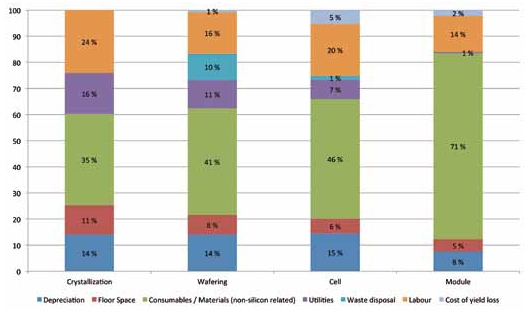
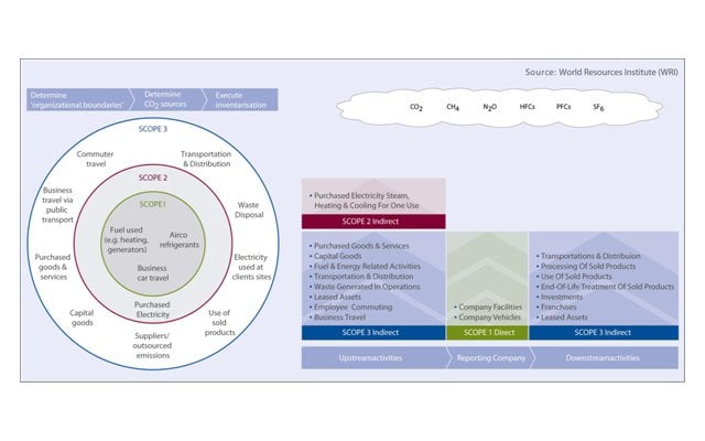
How much carbon is emitted in producing a solar PV module and launching it on the market? This could be an important question which project developers, installers, investors, government agencies and end customers might ask solar PV manufacturers in the future. To answer it, producers need to know the direct emissions from the manufacturing process, as well as those generated from the activities of manufacturers in the upstream supply chain (including raw material acquisition, upstream energy use, packaging, transportation and procurement), and also those arising from module usage and eventual recycling. This paper, written in a cooperation between EuPD Research and Deutsches CleanTech Institut (DCTI), presents an overview of PV’s carbon footprint.
Premium
Fab & Facilities, Photovoltaics International Papers
As the solar photovoltaic industry has matured from MW-scale pilot plants to large-scale mass manufacturing, costs of solar cells have steadily fallen. To further drive down costs of solar electricity beyond grid parity, a new approach that is being used is to investigate how photovoltaic manufacturing fits into the industrial ecology of a region. Optimizing the utilization of the waste associated with photovoltaic manufacturing itself and its components, while carefully considering geographic proximity, allows for industrial symbiosis. Industrial symbiosis engages traditionally separate industries in a collective approach to competitive advantage, involving physical exchange of materials, energy, water and/or by-products. Preliminary studies and industrial experimentation with co-production/co-location indicate that industrial symbiosis in photovoltaic manufacturing not only improves photovoltaic technology’s already stellar life-cycle environmental performance, but also provides for additional revenue streams that can be used to further reduce photovoltaic device costs. For example, simply coupling a glass manufacturing plant making substrates to a GW-scale amorphous silicon thin-film photovoltaic manufacturing plant, and using recycled glass where technically viable, can lead to a reduction of 30,000 tons/year in raw materials and a 12% reduction in embodied energy. Coupling the glass plant to a greenhouse to make use of waste heat means that more than 700 tons of tomatoes can be grown each year. Both these material and energy savings and additional revenue streams contribute to lowering photovoltaic manufacturing costs, which will play a progressively more important role in photovoltaic manufacturing at the large (>GW) scale.
Premium
Fab & Facilities, Photovoltaics International Papers
The low material cost and proven manufacturability of thin-film silicon has made this material very attractive for low-cost photovoltaics (PV). It is widely recognized that increasing the light-to-electricity conversion efficiency will play a critical role in expanding the acceptance of these products. The first commercial thin-film silicon solar cell consisted of a singlejunction structure using amorphous silicon; multijunction cells incorporating amorphous silicon and silicon germanium were later used to further improve efficiency. An even later development was the incorporation of nanocrystalline silicon as an active layer. This very interesting material, which consists of nanocrystallites embedded in an amorphous tissue, has already given rise to a significant increase in the performance of these multijunction cells. Most recently, some very innovative light-trapping concepts have been suggested that can improve the efficiency further. Both these topics, however, have required expertise not readily available within one organization. A thin-film silicon team has been established under a US Department of Energy’s Solar America Initiative programme to address the material, device and manufacturability issues for this technology. United Solar Ovonic is the team leader, with Colorado School of Mines, University of Oregon, Syracuse University and the National Renewable Energy Laboratory (NREL) as members. The collaborative effort has resulted in a new understanding of the material and devices; innovative light trapping ideas were developed, and worldrecord initial efficiencies of 16.3% for small-area cells and 12% for large-area encapsulated cells were reached. Of equal importance is United Solar’s decision to introduce this technology into production. This paper presents the important technical results obtained under this programme and will discuss future directions.

Subscribe to Newsletter

Upcoming Events

Solar Media Events
May 1, 2024
Dallas, Texas
Solar Media Events
May 21, 2024
Sydney, Australia
Solar Media Events
May 21, 2024
Napa, USA