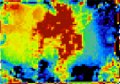
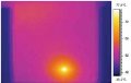
Technical Papers

Premium
Materials, Photovoltaics International Papers
Heat transfer and control of the temperature field are important in the production of silicon solar cell wafers. Present work focuses on the first steps of the production chain, i.e. crystallization and wafering. For the crystallization process, control of heat transfer is crucial for the ingot quality in terms of grain structure, impurity distribution, particle formation, and ingot stresses. Heat transfer is also important during subsequent processes, in particular the wire sawing of the silicon blocks into wafers. The paper emphasises the role of heat transfer and explains the consequences for these processes. Examples from experimental trials and measurements are combined with models and simulation methods.
Premium
Fab & Facilities, Photovoltaics International Papers
PV manufacturers can quickly reduce their costs, and increase their yields, by using SEMI standards that were originally designed to help semiconductor fabs deal with power glitches and power costs. SEMI, the global industry association serving the manufacturing supply chains for the microelectronic, display and photovoltaic industries, has two well-established electric power standards that could prove especially useful for PV manufacturing: SEMI F47, which helps equipment deal with power disturbances, and SEMI E3, which helps users understand how much electric power is used in their recipes. This paper provides a method of lowering costs and increasing yield by applying these standards in the PV manufacturing industry.
Premium
Photovoltaics International Papers, Thin Film
Chemical stoichiometry along with depth profiling and metallic contamination is of considerable interest for photovoltaic thin films. Conversion efficiency can be affected for example if primary components, e.g. Cd and Te, are not present at proper ratios. Moreover, amorphous silicon can vary substantially between sources and deposition technique, and qualitative comparison of trace metallic contaminants may not be sufficient to ensure final thin-film quality. This discussion presents data from atomic emission and mass spectrometry techniques that quantitatively and accurately describe both bulk and trace elemental compositions in photovoltaic materials, various thin-film matrices, and the final thin-film cell and module.
Premium
Cell Processing, Photovoltaics International Papers
This paper, the second in a series covering cost of ownership studies for photovoltaics [1], examines the need for saw damage removal and the follow-on processes of precleaning, texturization, and cleaning. The process considerations for wet and plasma approaches are further discussed before taking a detailed look at texturization using random pyramid formation. The paper will conclude with a view of current and future wet process techniques and a cost of ownership case study using Akrion Systems’ GAMA-Solar as an example.
Premium
Photovoltaics International Papers, PV Modules
Solar enterprises will each be faced with the occasional surplus or lack of solar modules in their lifetimes. In these instances, it is useful to adjust these stock levels at short notice, thus creating a spot market. Spot markets serve the short-term trade of different products, where the seller is able to permanently or temporarily offset surplus, while buyers are able to access attractive offers on surplus stocks and supplement existing supply arrangements as a last resort.
Premium
Materials, Photovoltaics International Papers
With growth in 2009 suffering from recession and an ongoing credit crunch, this paper presents a review of the key trends in cell and module manufacture for the crystalline silicon (c-Si) PV module market. The c-Si segment remains the largest segment, and is competing effectively with less mature thin-film technologies. PV is still a largely uneconomic way to generate power, and requires subsidy to maintain sales volume and growth. While subsidies exist, the industry treads the narrow path of growing at a healthy clip, developing robust technology and business models, and mapping paths to profitable business without subsidies once PV installations become economically viable.
Premium
Fab & Facilities, Photovoltaics International Papers
Development of fine-line crystalline silicon solar cells is a potential direction for application of high-efficiency and low-cost solar cells in the industry. Fine-line mask-free metallization offers huge potential to increase cell efficiency by reducing metal shadowing losses and surface recombination losses. At China Sunergy, three promising approaches for fine-line crystalline silicon solar cells are currently undergoing research, including processes such as laser doping selective emitter (LDSE) technology, inkjet or aerosol jet printing of metal paste and upgraded screen-printing technology. This paper presents the basic investigations of these three manufacturing technologies, singling out the technology that presents the most potential for further application.
Premium
Photovoltaics International Papers
After staying relatively quiet for much of the past year, thin-film PV manufacturer Nanosolar came out with a full docket of announcements on 9/9/09: the completion of its major panel-assembly factory near Berlin; the start of serial rollto-roll production of its flexible copperindium-gallium-(di)selenide cells in the company’s San Jose facility; $4.1 billion in panel purchases from customers – including some of the world’s largest utility companies; NREL-verified cell efficiencies up to 16.4%; and new technical details of both its printed CIGS cell technology and utility-scale panels.
Premium
Cell Processing, Photovoltaics International Papers
One-step screen-printing processes are still the most widely-used technique for the front-side metallization of crystalline silicon solar cells in the PV industry. This is because of the knowledge, stability and speed of the process, and despite some big disadvantages exhibited by the resulting contacts. Therefore, the metal contacts of high-efficiency laboratory cells are usually produced via advanced two-step metallization processes, which allow the application of optimized contact structures. In a first step, a narrow metal layer is applied to form the contact to the silicon wafer. Several different techniques have been developed for this first stage. In the second step, the seed layer is reinforced electrochemically with a dense layer of a metal of high conductivity, usually by light-induced plating. The transfer of such techniques into industrial scale has been pursued intensively, and may enter solar cell production lines in the near future. However, the process can still be improved based on a better process understanding, in order to benefit from the full potential of the technology.
Premium
Cell Processing, Photovoltaics International Papers
Standard solar cell technology nowadays offers a variety of measures - some linked, some not - to continuously improve conversion efficiency. The starting point for considering the different improvement steps is a kind of standard cell as produced on most current production lines. The main elements of this cell are diffused junction, aluminium back-surface field and screen-print metallization. This type of cell suffers losses from different sources like optics, recombination and resistance that can be considerably lowered to obtain higher cell efficiency. This paper will describe improvement steps on the standard type of multi-crystalline cell before addressing cell concepts that open further potential.

Subscribe to Newsletter

Upcoming Events

Solar Media Events
May 1, 2024
Dallas, Texas
Solar Media Events
May 21, 2024
Sydney, Australia