
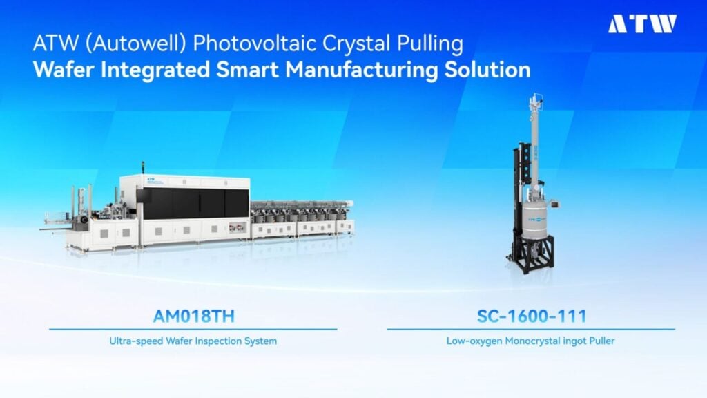
Autowell (ATW)’s PV crystal pulling–wafer integrated smart manufacturing solution combines end-to-end automation, AI-driven crystal pulling, precision sorting and big-data analytics to reduce oxygen content, improve minority carrier lifetime and lower breakage rates, helping customers enhance quality and profitability amid the P-to-N transition and overcapacity. Backed by full-lifecycle services, the solution enables robust digital transformation for PV manufacturers.
The global PV industry is undergoing a technology transition from P‑type to N‑type cell architectures, while shifting its strategic focus from capacity expansion to efficiency‑driven quality improvement. According to China’s Photovoltaic Industry Association (CPIA), global installations reached some 580 GW in 2025, with the N‑type wafer market share exceeding 70%. This imposes stricter requirements on oxygen content, minority carrier lifetime and defect control. Meanwhile, wafer sizes continue to expand (from 182mm to 210mm) while thickness decreases (below 130μm), intensifying challenges related to breakage rates, yield and silicon consumption. In this context, ATW, leveraging its full‑chain equipment capabilities covering crystal pulling, wafer, cell and module segments, has launched its new smart manufacturing solution, built on automation, informatisation, and customised services to help customers address both quality and cost pressures.
ATW’s solution rests on the three integrated pillars of seamless physical‑layer automation, centralised information‑layer control and customizable service‑layer delivery, covering the entire workflow from polysilicon material to qualified wafer outbound.
The company’s third‑generation single‑crystal furnaces employ AI‑based vision and thermal‑field models to automate charging, seeding, shoulder growth, constant‑diameter growth and tailing, significantly reducing manual intervention, proprietary thermal‑field design and heating strategies maintaining oxygen content at 6–7 ppm. Feedback from multiple leading cell manufacturers indicates that 36‑inch N10/N12 wafers produced with ATW’s pulling process show minority carrier lifetime improvements of approximately 15% and 20%, respectively, corresponding to cell efficiency gains of 0.1–0.2 percentage points. The system incorporates dual‑redundant monitoring of liquid‑level gap and load cells, water‑cooling screen leak detection, software interlocking and silicon leakage alarms to ensure sustained stable operation.
ATW’s crucible charger completes a cycle in 12 minutes and can serve up to 700 furnaces per unit; the barrel charger completes a cycle in 4 minutes and serves up to 160 furnaces. The OCZ external charger has a 500 kg capacity, enhancing furnace productivity by approximately 5%.
The automatic crystal extraction vehicle handles crystal lengths from 1,500 mm to 7,000 mm with a load capacity exceeding 850 kg, and completes a full extraction cycle in less than 20 minutes, saving 5 to 10 minutes per cycle compared to conventional methods. The system requires only one operator for initial confirmation and can thereafter run unattended, with a single vehicle serving up to 60 furnaces, improving extraction efficiency by approximately 30%.
The automatic hot‑zone cleaning robot handles loads of up to 180 kg with ±4 mm vision positioning accuracy, improving efficiency by approximately 50% compared with manual cleaning, enhancing hot-zone installation consistency, reducing labour intensity and minimising downtime.
The ATW AM018TH high‑speed sorter integrates multi‑modal inspections covering dimensions, thickness, contamination, edge chipping, resistivity, cracks, P/N type and holes. Overall sorting efficiency improves by over 30% compared to conventional models, with dual‑track independent operation doubling capacity without increasing footprint and compatible with full and half cells, maintaining breakage rates stably below 0.03%. The G018TH model is optimised for ultra‑thin wafers and high‑resistivity detection, with options for stack re‑run and fixed‑point collection. Inspection modules feature:
- Cracks: 1300nm IR with InGaAs sensor, stereoscopic imaging distinguishes cracks from surface stains;
- Contamination: Full coverage of linear, scattered and clustered irregularities;
- Edge chipping: Blind‑spot‑free scanning along edges and chamfers, including inner and outer corners;
- Holes: Dual 8K line‑scan cameras with optimised lighting enhance contrast for micro‑defect detection.
The ATW analytics platform generates full‑ingot defect heatmaps with positioning accuracy ≤500 μm, and employs clustering algorithms to automatically classify defect types for process traceability. Independent left‑centre‑right wire mark and thickness analysis (1 mm accuracy) quantifies the proportion of various wire mark types and correlates TTV trends to pinpoint root causes. AI models predict the remaining useful life of critical components and automatically push maintenance tasks, while supporting customizable checklists to accommodate diverse production line maintenance strategies.
The ATW solution supports direct MES integration with cell production lines and complies with ETL and SES/GEM communication standards for seamless data interconnection. The automated re‑inspection and packaging line performs final checks on breakage, chipping, contamination, bagging quality and push pressure to ensure outbound quality.
The company assigns dedicated project teams to provide closed‑loop services — from early‑stage process evaluation and solution design, through equipment selection, layout planning and automation customisation during implementation, to installation, commissioning, training and a 1‑year warranty period. Customers benefit from on‑site rapid response and regular process review visits to drive continuous efficiency improvement.
The solution has already been deployed at multiple leading domestic PV manufacturers. Operational data demonstrates effective oxygen content control, improved minority carrier lifetime, increased sorting efficiency, reduced breakage rates and optimised process parameters through digital twin and big data integration. As N‑type penetration continues to rise and global installation demand grows steadily, smart manufacturing is becoming an increasingly important pathway for PV companies to enhance competitiveness. ATW will continue to deepen its technological integration across digital twins, AI inspection and big data analytics, delivering more efficient and reliable smart factory solutions to global customers.