On November 27th, Trina Solar, Risen Energy, Zhonghuan Semiconductor, Tongwei, Huansheng Photovoltaic, Runyang New Energy Technology, Canadian Solar and Wuxi Shangji Automation jointly proposed standardization on the 210mm silicon wafer and module size for the photovoltaic industry. The eight companies’ proposal followed the SEMI standard within the 210-220mm size range: 210+/-0.25mm as the only size, at the same time revising the SEMI and existing module sizes in the PV industry association.
Advantages of the larger size and comparison of price-performance ratio
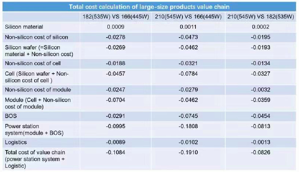
Since 2019, cost reduction in the photovoltaic industry has entered a new stage, with larger size silicon wafers, cells and modules. The benefits of high-power modules are well-known: flux value, dumpling effect and cost savings on a number of elements that drive cost reduction in large-size wafers, cells, modules and BOS.
Flux value refers to the increase in production capacity brought about by large-size products, thereby reducing the cost of labour, depreciation, and three types of other expenses (operating, management and financial) per unit of output. The ‘dumpling’ effect refers to the increase in the amount of auxiliary materials in transportation such as frame, glass, backsheet, EVA, ribbon bus bars, pallets and packaging materials being less than the increase in module area when using large-size wafers in module production, bringing savings in encapsulation and transportation costs. Cost savings related to the number of elements refers to the process of module production and power station construction where junction box, potting, combiner box, DC cable, installation and construction costs are directly related to the number of modules, so the use of larger-size products will increase module area and power and significantly decrease module production per watt and power station construction costs.
The significance of standardization of the 210mm size silicon wafer
Standardization of the 182mm size first occurred in June. At that time, only the silicon wafer size was defined, and the module size that ultimately reflected customer value was not considered. From the product specifications of the three main module manufacturers, the module sizes were 2274*1134; 2256*1133; 2285*1136. This time, the 210-camp represented by Trina Solar proposes standardization of the advanced 210mm size, including specifications and recommendations for the size of silicon wafers and module design (whether glass-glass or backsheet),suggesting no other sizes should be used in the range of 210mm-220mm.
What is the cost reduction effect of standardization of the 210mm size?
Through standardization of the 210mm size silicon wafer and module, the industrial chain can achieve the best economy of scale. This can help upstream and downstream companies to significantly improve production efficiency, optimize supply and drive industry technological innovation, while reducing the cost of industry chain manufacturing, the initial investment in photovoltaic systems and LCOE (levelized cost of energy) of power generation, in order to achieve grid parity.
The 210mm wafer and module size standardization proposition is the first-ever attempt by the industry to standardize the entire industry chain, including module products. This initiative is not only from the perspective of the industry chain, but also from the standpoint of users. A unified module size effectively solves the pain point for customers, greatly reducing uncertainty in the design process, improving efficiency when selecting racking structures, inverters, cables and combiner boxes and enhancing the flexibility of module supply. At the same time, the installation efficiency for modules and racking structures can be improved and design and EPC costs reduced.
Following standardization on size, when an investor has multiple power stations under construction and the supply of modules for all cannot be guaranteed, there will be greater supply flexibility. The owner can have flexible deployment between projects or between each bidding section of a project according to the degree of urgency, without affecting the grid connection schedule.
Standardization on size can also ensure consistency of mounting holes during racking structure design, effectively speeding up the design and processing progress of the racking structure and providing a guarantee of rapid advancement of an owner’s project. In this way, the versatility of the racking structure is improved and, should project capacity have to be reduced due to external reasons, the racking structure purchased by the owner will not be wasted and can be used for other projects.
The value of standardization is also reflected in the development, operation and maintenance of a power station, being conducive to the reduction of spare parts (modules, fuses, cables) on-site and facilitating operation and maintenance management. It is additionally more user-friendly and versatile for projects that are planning to use automatic cleaning robots for arrays. It ensures accuracy during installation and can reduce rework and damage/impact on module performance.
The ongoing cost reduction in the photovoltaic industry and the increase in competitiveness of the price of solar storage power per kilowatt-hour will inevitably be accompanied by standardization in the future. Based on the significant advantages of the 600W+ ultra-high power module system, a standardized module size will bring more long-term value to customers in the design of downstream power stations.
From the perspective of supply, standardization is beneficial in improving its stability and reducing the cost of the overall industrial chain. Upstream and auxiliary materials such as glass, silicon wafers and junction boxes would be produced under unified standards, which would greatly reduce losses caused by switching production lines and inventory costs due to different specifications. Production within the 210 mm module’s entire industry chain would therefore be more orderly and effective.
The diversification in module sizes has not only resulted in low matching of supply chains, but also added a lot of direct and hidden costs. Many glass and module manufacturers have put forward their demands for uniformity in specifications as far as possible. When glass supply becomes tight, the industry still loses more than one million square meters of glass production capacity every month due to the switch to different sizes in product specifications, and hundreds of thousands of square meters of glass have become ‘stranded’ inventory due to the cancellation of customer orders. Not only that, the diversification in the size of modules has forced glass manufacturers to stock a variety of specifications, since one cannot necessarily be used between different module factories. This means that glass companies incur significant additional inventory costs, affecting their supply capacity and ability to deliver on time. Standardization on size would mean the inventory and supply of glass and all other materials could be optimized.
Production and manufacturing processes in the overall industrial chain, including silicon wafer pulling, slicing, cell manufacturing and module manufacturing would also be positively impacted by standardization. Even if manufacturing equipment is compatible, different tooling and fixtures currently have to be configured to meet varying cell or module sizes (tooling cost is estimated at 5-7 million RMB/GW). The greater impact, however, is the loss of production capacity when switching between products of different specifications and the processing costs for downgraded products. According to preliminary estimates by industry insiders, it usually takes 10-12 hours to switch between different products in cell and module manufacturing. In addition to the loss of yield and efficiency per switch, the cost of each is about 0.003-0.005¥/W, with its corresponding 1GW cost of 3-5 million¥/run.
Compared with previous products, the 210mm size module and related system solutions based on the new technology platform have significant advantages in terms of materials, design, process and system. With the standardization on large size silicon wafers, solar cells, and module sizes, the industry chain will achieve a better scale effect, improve production efficiency, and reduce the cost of industrial chain manufacturing, initial system investment and LCOE of power generation. Through the unification of standards, the entire industry chain can work together to create higher-quality photovoltaic products, bring higher value to customers, and reduce the LCOE of power generation. This standardization initiative is of great significance to the photovoltaic industry and will lead the industry to a new level.