Technical Papers

Premium
Photovoltaics International Papers, Power Generation
As it makes its way towards a non-subsidised market, the photovoltaic sector has to deal with decreasing margins. To ensure investment goals are met in spite of this, it is imperative that PV power plants generate optimal yields. Comprehensive quality assurance for PV power plants covers all phases of the completion process from the planning to system operation. This article explains the extent of standard quality assurance measures that include yield assessments, module measurements, system testing and yield monitoring. It outlines the potential of linking these quality assurance measures and stresses the importance of the measures themselves being of high quality. Up-to-date scientific findings from Fraunhofer ISE are presented in order to further optimise quality assurance measures.
Premium
Cell Processing, Photovoltaics International Papers
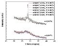
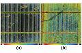
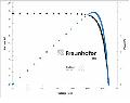
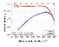
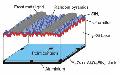
A hydrogenated amorphous Si (a-Si:H) film, combined with a silicon nitride (SiNx:H) capping layer and a post-deposition anneal, can hugely enhance the surface passivation on crystalline silicon wafers. In this work, the influence of various deposition temperatures of a-Si:H films on the thermal stability of a-Si:H/SiNx:H stacks and a possible mechanism are discussed. Both minority carrier lifetime measurement and grazing-angle XRD were employed to study the thermal stability of a-Si:H/SiNx:H stacks, and the results are interpreted in terms of dihydrides concentration and epitaxial crystallization. With an appropriate thermal treatment, the a-Si:H film deposited at 130°C and capped by SiNx:H showed better passivation performance than 200°C-deposited a-Si:H/SiNx:H stacks, but under an excessive thermal budget the former showed more severe degradation of carrier lifetime. The more dihydride-rich composition within 130°C-deposited a-Si:H/SiNx:H stacks could be regarded as providing more effective intermediates for hydrogen interchanges, but on the other hand, it is also more susceptible to epitaxial crystallization.
Premium
Cell Processing, Photovoltaics International Papers
A selective emitter is a doping layer that is heavily doped beneath the electrode and lightly doped in between the electrode grids. One of the disadvantages of conventional selective-emitter techniques is the need for a high phosphorus surface concentration to obtain low contact resistance and limit the shunts in the emitter. Effective emitter passivation below the contact is difficult because of the use of emitters with low sheet resistances and high doping concentrations. In this study, the selective emitter in the optimized light/light sheet-resistance combination was formed to reduce recombination under the metal contact. The fabrication of optimized light/light doped emitters was performed using a single-step diffusion process. Besides the benefit of low surface recombination for light/light combination, this approach also removes the need for a very precise alignment between the opened emitter pattern and the front screen-printed silver fingers. This work illustrates the achievement of an efficiency improvement of more than 0.4% absolute in large-scale production for selective emitter solar cells.
Premium
Cell Processing, Photovoltaics International Papers
The workhorse of the photovoltaic industry, crystalline-silicon solar cells, continues to have additional headroom for conversion efficiency improvement as well as decreased production costs. As some companies have already demonstrated, clear pathways exist to bring about the achievement of >20%-efficient monocrystalline cells through the use of existing and novel production techniques. A newcomer to the solar cell and module sector, Suniva, has rapidly become a volume manufacturer using innovations originally developed at the University Center of Excellence in Photovoltaics (UCEP) at the Georgia Institute of Technology. This paper discusses the company’s first- and second-generation production technologies, including the implementation of ion implantation as a high-volume process, as well as details of cell-making approaches in the development stage.
Premium
Cell Processing, Photovoltaics International Papers
Laser grooved buried contact (LGBC) solar cell technology is proving to be an attractive method of producing solar cells that are designed to operate at one sun and at concentration. Such technology is commercially available at Narec for applications at up to 100 suns. Although LGBC cells can have a higher efficiency at one sun when compared with standard non-selective emitter screen-printed solar cells, a more complex manufacturing process is required for these cells. This paper outlines the approach taken under the FP6 EU funded project “Lab2Line”, in which screen-printing and LGBC solar cell processing techniques are hybridized in order to produce lower cost, high efficiency solar cells.
Premium
Fab & Facilities, Photovoltaics International Papers
The recent 30% decline in module market prices is the most telling sign of a need for continuous reductions in PV production costs. With this in mind, the cost efficiency of production processes is, next to stable product quality, a vital objective in the planning of production facilities. In this paper, the lessons learned in the area of cost of ownership (COO) forecasting methodologies will be analyzed and evaluated for their potential application to investment decisions in the PV industry. This paper will analyze the cost structure of the PV industry with the aim of underlining the importance of a systematic cost-of-ownership approach.
Premium
Fab & Facilities, Photovoltaics International Papers
A major challenge for the solar industry over the next few years is the reduction of production costs on the road to grid parity. Capacity must be increased in order to leverage scaling effects, production and cell efficiency must also be enhanced, and the industry must focus on intensified process optimization and quality control. Laser marking can make a key contribution to fulfilling these requirements. As hard physical coding, laser marking is applied to the raw wafer at the start of the manufacturing process, making each solar cell traceable along the entire value chain and over its whole lifetime. This paper presents Q-Cells’ laser-supported process for coding each individual solar cell (European patent pending), which will require transition work at the laboratory stage before the company’s innovation is ready for mass production.
Premium
Market Watch, Photovoltaics International Papers
The U.S. solar PV market is suffering not from a lack of demand or high prices, but rather from an inconsistent labyrinth of rules and regulations which complicate and prolong uptake. There is significant pent-up demand in the U.S. among developers and especially manufacturers; there is not, however, a commensurate regulatory framework that will enable and encourage this demand to be realized. The U.S. political landscape is deeply divided, and policies that would directly or indirectly effect solar demand are no different from any other in this regard.
Premium
Materials, Photovoltaics International Papers
The minority carrier lifetime is a key parameter for the performance of solar cells as it characterizes the electrical quality of the semiconductor material. Consequently, accurate and reliable methods to determine the minority carrier lifetime are of enormous interest for both practical process control and the evaluation of the potential and limitations of a specific cell concept. Due to its importance, many different lifetime measurement techniques have been developed and used over the past few decades. This paper aims to present and discuss the most common measurement methods on the one hand, while attempting to shed light on some recent developments on the other. The determination of the minority carrier lifetime of crystalline silicon thin-film (cSiTF) material is illustrated as an example of interest for those who are already familiar with standard lifetime characterization.
Premium
Materials, Photovoltaics International Papers
The next generation of industrial silicon solar cells aims at efficiencies of 20% and above. To achieve this goal using ever-thinner silicon wafers, a highly effective surface passivation of the cell, front and rear, is required. In the past, finding a suitable dielectric layer providing a high-quality rear passivation has been a major challenge. Aluminium oxide (Al2O3) grown by atomic layer deposition (ALD) has only recently turned out to be a nearly perfect candidate for such a dielectric. However, conventional ALD is limited to deposition rates well below 2nm/min, which is incompatible with industrial solar cell production. This paper assesses the passivation quality provided by three different industrially relevant techniques for the deposition of Al2O3 layers, namely high-rate spatial ALD, plasma-enhanced chemical vapour deposition (PECVD) and reactive sputtering.

Subscribe to Newsletter

Upcoming Events

Solar Media Events
May 21, 2024
Sydney, Australia
Solar Media Events
May 21, 2024
Napa, USA
Solar Media Events
May 22, 2024
London, UK
Upcoming Webinars
May 29, 2024
11am (EDT) / 5pm (CEST)