By Zhenggang Yang, PV Module Technical Support Engineer, ET Solar Group
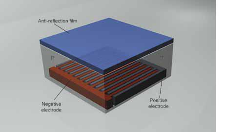
A new production process for crystalline silicon (c-Si) solar cells, specifically p-type back-contact solar cells, is proposed. In contrast to the conventional c-Si solar cell manufacturing method, this new technology eliminates the etching process and reduces the industrial three-step electrode printing to only one step, greatly improving the technological process. Furthermore, the proposed process is also largely compatible with a traditional c-Si solar cell production line. Oxidation technology for producing the SiO2 film on a c-Si wafer, together with corrosive window technology, such as through HF corrosive paste screen printing, for creating the patterning on the wafer covered with SiO2 film, are used in the fabrication of the p-type back-contact solar cells.