By Frédéric Dross, Research Engineer & Team Leader, IMEC; Kris Baert, Programme Manager of Solar Cells, SOLO Department, IMEC; Jef Poortmans, Program Director, Strategic Programme SOLAR+ and Department of Solar and Organic Technologies, IMEC
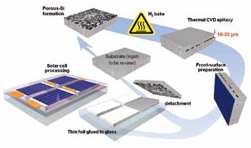
Today, crystalline-Si photovoltaics (PV) dominate the market, accounting for more than 85% of market share in 2010. A large scientific community made up of academic as well as industrial stakeholders strives to find solutions to improve device efficiencies and to drive down costs. One of the important cost elements of a module is the c-Si wafer itself. This paper discusses the fabrication of a carpet of c-Si foils on glass, either by layer transfer of an epitaxially-grown layer or by bonding of a very thin wafer, and processing this c-Si thin-foil device into a photovoltaic module. This could constitute an advantageous meet-in-the-middle strategy that benefits not only from c-Si material quality but also from thin-film processing developments.