Requires Subscription: Photovoltaics International Archive

Current topics in CIGS solar cell R&D - Part 2: Buffer layers and metastabilities in CIGS

Facebook
Twitter
LinkedIn
Reddit
Email

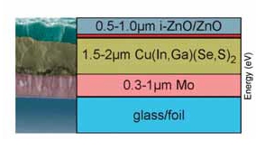
By Niklas Papathanasiou, Head of CIGS Solar Cell Development, Helmholtz-Zentrum Berlin für Materialien und Energie GmbH/PVcomB

This is the second part of a review article series about current topics in R&D concerning Cu(In,Ga)(Se,S)2 – or CIGS – solar cells. In the first part, which appeared in the previous edition of Photovoltaics International, the focus was on CIGS absorber layer formation. This second part will discuss another essential part of CIGS solar cells – the buffer layer – in conjunction with metastabilities in these types of cell.

L3dwLWNvbnRlbnQvdXBsb2Fkcy9sZWdhY3ktcHVibGljYXRpb24tcGRmcy9jNDFiMjJkNWM3LWN1cnJlbnQtdG9waWNzLWluLWNpZ3Mtc29sYXItY2VsbC1yZC1wYXJ0LTItYnVmZmVyLWxheWVycy1hbmQtbWV0YXN0YWJpbGl0aWVzLWluLWNpZ3MucGRm

Published In

Photovoltaics International Archive
For manufacturers who had their heads in the bunker during 2012, fighting falling ASPs and eroding margins, the nineteenth edition brings you details of what lies in store for this coming year. Wright Williams & Kelly return in this issue with their popular analysis of payback on technology buys; crucially they analyze n-type wafers, Al2O3 passivation and copper metallization. SERIS shows us how to achieve 18.7% efficiencies using low-cost etching techniques on diffused wafers. We also have two important technology roundups: CIGS from Helmholtz Berlin, and PV module encapsulation techniques from Fraunhofer ISE.

Read Next

Subscribe to Newsletter

Most Read

Upcoming Events