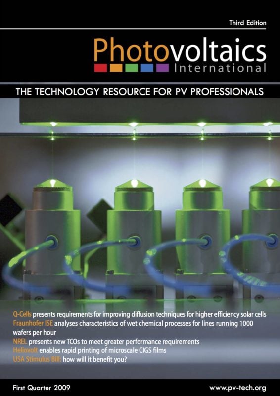
By Stefan Peters, Department for Thermal and Vacuum Processes, Q-Cells SE
Formation of the pn-junction for charge carrier separation is one of the key processes of a modern high-volume solar cell production. In silicon wafer-based solar cell technology this is achieved by diffusion of phosphorus atoms in boron pre-doped wafers forming a sub-micron shallow n-type emitter in a 200µm-thick p-type base. In this contribution we discuss both the characteristics of emitter doping profiles and the diffusion process itself as required for optimal solar cell conversion efficiencies. In addition we give an overview on state-of-the-art industrial diffusion technologies and conclude with a brief outlook on their evolution.


