By Dorit Linaschke, Researcher and Project Manager in the CVD Thin-Film Technology Group, Farunhofer IWS; Gerrit Mäder, Project Manager, Farunhofer IWS; Wulf Grählert, Leader of the Process Monitoring Group, Farunhofer IWS; Ines Dani, Head of the Atmospheric Pressure CVD Group, Farunhofer IWS; Mattias Leistner, Staff Member at the Process Monitoring Group, Farunhofer IWS; Stefan Kaskel, Head of the CVD and Thin Film Technology Department, Farunhofer IWS
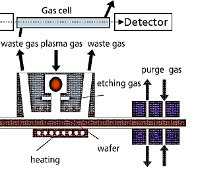
The etching technology currently used in the solar industry is mostly based on wet chemical processing. Plasmaenhanced dry chemical etching at atmospheric pressure is an alternative to the existing technology, especially when combined with similar process technologies, for example plasma-enhanced deposition techniques at atmospheric pressure, to provide a continuous in-line processing of crystalline silicon solar cells. This paper presents the use of plasma chemical etching using Fourier Transform infrared (FT-IR) spectroscopy to monitor different silicon wafer processing steps as an alternative to the widely used wet chemical processing approach.