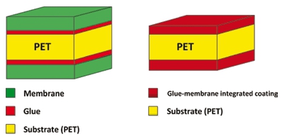
Technical Papers

Premium
Fab & Facilities, Photovoltaics International Papers
As the solar photovoltaic industry has matured from MW-scale pilot plants to large-scale mass manufacturing, costs of solar cells have steadily fallen. To further drive down costs of solar electricity beyond grid parity, a new approach that is being used is to investigate how photovoltaic manufacturing fits into the industrial ecology of a region. Optimizing the utilization of the waste associated with photovoltaic manufacturing itself and its components, while carefully considering geographic proximity, allows for industrial symbiosis. Industrial symbiosis engages traditionally separate industries in a collective approach to competitive advantage, involving physical exchange of materials, energy, water and/or by-products. Preliminary studies and industrial experimentation with co-production/co-location indicate that industrial symbiosis in photovoltaic manufacturing not only improves photovoltaic technology’s already stellar life-cycle environmental performance, but also provides for additional revenue streams that can be used to further reduce photovoltaic device costs. For example, simply coupling a glass manufacturing plant making substrates to a GW-scale amorphous silicon thin-film photovoltaic manufacturing plant, and using recycled glass where technically viable, can lead to a reduction of 30,000 tons/year in raw materials and a 12% reduction in embodied energy. Coupling the glass plant to a greenhouse to make use of waste heat means that more than 700 tons of tomatoes can be grown each year. Both these material and energy savings and additional revenue streams contribute to lowering photovoltaic manufacturing costs, which will play a progressively more important role in photovoltaic manufacturing at the large (>GW) scale.
Premium
Fab & Facilities, Photovoltaics International Papers
The low material cost and proven manufacturability of thin-film silicon has made this material very attractive for low-cost photovoltaics (PV). It is widely recognized that increasing the light-to-electricity conversion efficiency will play a critical role in expanding the acceptance of these products. The first commercial thin-film silicon solar cell consisted of a singlejunction structure using amorphous silicon; multijunction cells incorporating amorphous silicon and silicon germanium were later used to further improve efficiency. An even later development was the incorporation of nanocrystalline silicon as an active layer. This very interesting material, which consists of nanocrystallites embedded in an amorphous tissue, has already given rise to a significant increase in the performance of these multijunction cells. Most recently, some very innovative light-trapping concepts have been suggested that can improve the efficiency further. Both these topics, however, have required expertise not readily available within one organization. A thin-film silicon team has been established under a US Department of Energy’s Solar America Initiative programme to address the material, device and manufacturability issues for this technology. United Solar Ovonic is the team leader, with Colorado School of Mines, University of Oregon, Syracuse University and the National Renewable Energy Laboratory (NREL) as members. The collaborative effort has resulted in a new understanding of the material and devices; innovative light trapping ideas were developed, and worldrecord initial efficiencies of 16.3% for small-area cells and 12% for large-area encapsulated cells were reached. Of equal importance is United Solar’s decision to introduce this technology into production. This paper presents the important technical results obtained under this programme and will discuss future directions.
Premium
Photovoltaics International Papers, Thin Film
In situ, real-time and off-line polarization spectroscopies have been applied in studies of large-area spatial uniformity of the components of multilayer stacks in hydrogenated silicon (Si:H) and cadmium telluride (CdTe) thin-film photovoltaic (PV) technologies. Such reflection spectroscopies involve first the measurement of spectra in the reflected-to-incident polarization state ratio of the light wave (or the ellipsometry angles of the reflecting multilayer stack), and then the analysis of these spectra to determine the thicknesses and properties of component layers of the stack. In addition, expanded capabilities result from measurement/analysis of the irradiance ratio and the degree of polarization of the reflected beam, simultaneously with the polarization state ratio, particularly for rough surfaces with in-plane roughness scales of the order of the optical wavelength or greater that scatter and depolarize the light beam. This paper provides examples of 1) real-time monitoring of texture etching of the transparent conducting oxide ZnO:Al; 2) real-time monitoring and off-line mapping of roll-to-roll deposited hydrogenated amorphous silicon (a-Si:H); and 3) large-area mapping of coated glass panels used in low-cost CdTe PV technology. For a-Si:H and CdTe thin-film PV technologies, the focus is on the characterization of the window layers, which are p-type protocrystalline Si:H and n-type cadmium sulphide (CdS), respectively. Analysis of the thickness, phase and structure of the window layer material over the area of the PV panel is critical in order to design processes for uniformity of high performance. Descriptions are given of future directions in novel instrumentation development that will enable mapping for uniformity evaluation at the high speeds required for on-line analysis.
Premium
Photovoltaics International Papers, PV Modules
By definition, PV module certification is simply based on conformance to standards. The IEC norms for PV modules are considered to be adequate quality requirements for guaranteeing initial quality. However, it is commonly understood that two products A and B may meet the standard’s requirements, but overall qualty – considering long-term stability, performance and safety – can still be quite different. PV module testing should therefore be carried out more frequently and beyond IEC requirements. A factory inspection once a year – as suggested by most certification bodies to ensure continuous quality of certified crystalline modules – may not be sufficient. The need for additional control is demonstrated in this paper, with reference to our experience from PV module testing and quality assurance activities for wholesalers and project developers. We present the necessity of additional measurements under standard test conditions (STC) and advanced testing methods, which are becoming essential for reliability.
Premium
Cell Processing, Photovoltaics International Papers
Approximately 80% of today’s silicon solar cells industrially manufactured worldwide apply screen printing for the metallization of the silver front and aluminium rear contacts. In production, conversion efficiencies of ~18–18.5% are achieved using monocrystalline silicon wafers. A baseline process has been implemented at ISFH that is very similar to the industry-standard process, displaying conversion efficiencies of up to 18.5%. An analysis of the solar cells reveals that the conversion efficiency is limited in particular by the shadowing loss due to the silver front-side metallization, as well as infrared light being absorbed in the aluminium rear-side metallization. This paper summarizes recent developments at ISFH that resulted in a 19.4% efficient large-area screen-printed solar cell, when applying a print-on-print silver front-side metallization and an SiO2/SiNx rear-surface passivation.
Premium
Materials, Photovoltaics International Papers
Competition in the premium sector is becoming more and more fierce. This is forcing PV module manufacturers to differentiate themselves through product benefits and better performance in terms of efficiency. While attention has previously been focused on cell technology, it is likely that, in the future, all module components will become part of this competition – a competition in which premium front glasses present an especially promising element. Antireflective coating (ARC) is only the beginning of this evolution. Not only do deeply textured front glasses promise significant increases in output – up to 7% – but their specific product characteristics also make them suitable for niche applications, such as airplane entry lanes and airport buildings. EuPD Research has issued a white paper devoted to solar glass, of which a synopsis is presented here.
Premium
Photovoltaics International Papers, Thin Film
Transparent conductive oxides (TCOs), such as aluminium-doped zinc oxide (ZnO:Al), play an important role in thin-film photovoltaics. As a material for front contacts, ZnO:Al is standard in industrial-scale production, especially in the field of Cu(In,Ga)Se2 solar cells. Over the last few years, there has been a strong push to use ZnO:Al films on glass as substrates for amorphous or amorphous/microcrystalline silicon solar cells, and these films have now been introduced as an alternative to the typically used fluorine-doped tin oxide (SnO2:F) films in production. Sputtering coaters for large area deposition of ZnO:Al are widely available, and ZnO:Al films are produced in these coaters by sputtering of ceramic targets. This technology offers high process stability and is therefore favoured over reactive sputtering of metallic targets. With respect to cost and quality, however, the reactive process is an interesting alternative. In this paper we will give an overview of the process of reactive sputtering of ZnO:Al and discuss the most important insights.
Premium
Cell Processing, Photovoltaics International Papers
In a multicrystalline silicon (mc-Si) cell production process, acid texturing is the most popular way of carrying out surface texturing. In general, the surface reflectivity and etch depth are the criteria used for quantifying the texture quality. In this study, four groups of cells were created with different etch depths of 2.82μm, 3.83μm, 4.41μm and 5.92μm. It was found that the etch depth had a notable effect on the efficiency of a cell. Also, the best texture was obtained with an etch depth of 4.41μm, at which there was a balance between a low reflectance and the removal of the saw-damage layer. As the etch depth increased, the film deposition thickness and the front bus-bar tensile strength were seen to increase. However, no linear relationship was found to exist between the diffusion sheet resistance and the etch depth.
Premium
Materials, Photovoltaics International Papers
The last several years have seen a significant number of publications on wire saw data in regard to process optimization theory applied to solar wafering. The methods vary, but fundamentals concern the mechanical dynamics of the wire sawing process, where measurements of the wire forces in the silicon slot using free abrasive are studied; however, these data are not yet fully correlated to a complete thermodynamic analysis of the problem. The objectives of the empirical development of the process theory are also widely varied, but there is industry agreement that it is being faced with the fundamental limits of cutting rates in processes that use free abrasive slurries and a single wire. The limit arises from intrinsic thermodynamic limits of the delivery of work energy to the silicon slot. Similarly, these same principles prevent us from increasing the wafer load to overcome the limitation as work energy transfer rates are countered by higher entropic losses that occur as power and wafer load are increased. The effect results in the problem that the wafer load may not be increased without proportionately reducing table speed. The fundamental nature of these limits suggests that they involve theoretically calculable energy quantities of thermodynamic limiting functions, which restrict the ‘useful’ work that we can extract from the system, where the work energy of interest is the abrasion of the silicon in forming the wafers. The present work reviews the theoretical issues of determining process efficiency optimums that could be used to achieve throughput gains.
Premium
Photovoltaics International Papers, PV Modules
Solar enterprises will each be faced with the occasional surplus or lack of solar modules in their lifetimes. In these instances, it is useful to adjust stock levels for modules at short notice, thus creating a spot market. Spot markets serve the short-term trade in different products, where the seller is able to permanently or temporarily offset surplus, while buyers are able to access attractive offers on surplus stocks and supplement existing supply arrangements as a last resort.

Subscribe to Newsletter

Upcoming Events

Solar Media Events
May 1, 2024
Dallas, Texas
Solar Media Events
May 21, 2024
Sydney, Australia
Solar Media Events
May 21, 2024
Napa, USA