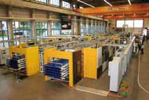
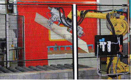
Technical Papers

Premium
Photovoltaics International Papers, PV Modules
Solar enterprises will each be faced with the occasional surplus or lack of solar modules in their lifetimes. In these instances, it is useful to adjust these stock levels at short notice, thus creating a spot market. Spot markets serve the short-term trade of different products, where the seller is able to permanently or temporarily offset surplus, while buyers are able to access attractive offers on surplus stocks and supplement existing supply arrangements as a last resort.
Premium
Photovoltaics International Papers, PV Modules
Over the past few decades, the PV equipment manufacturing market has seen a significant change in technologies. Cell sizes are being increased, while cell thickness has decreased at an ever-increasing speed of technological innovation, from 4” 340µm cells in the 1990s to 6”+ 180µm being the current industry standard. Thin-film modules pose completely new challenges to module manufacturing technology with a strong integration of the manufacturing of the active layers into the module production flow. This articles analyses the pros and cons of an increased level of line integration from the viewpoint of an established PV module producer.
Premium
Cell Processing, Photovoltaics International Papers
Explosive growth in sales of critical subsystems and components for use in photovoltaic manufacturing equipment provided one of the few bright spots in an otherwise depressed market during 2008. The outlook for sales into the PV industry in 2009 is for demand to be relatively flat, but strong underlying demand for PV cells should lead to a recovery in 2010 and a return to double-digit growth rates, as outlined in this paper.
Premium
Photovoltaics International Papers, Power Generation
Thin-film or crystalline photovoltaic modules? One of the consequences of the rapid introduction of new photovoltaic technologies is the buzz generated in the industry. Large-scale photovoltaic applications are especially sensitive to any question connected with cost optimization. Therefore, stakeholders involved in photovoltaic project development are questioning whether the time has arrived to shift module technologies to large-scale applications. A great variety of opinions are exposed every time this question arises. This paper’s aim is to uncover the key questions that should be taken into consideration in order to select the proper technology for large-scale photovoltaic applications and to provide the maximum amount of practical information for this decision.
Premium
Market Watch, Photovoltaics International Papers
In 2008, the global PV market reached 5.6GW and the cumulative PV power installed totalled almost 15GW compared to 9GW in 2007. Spain represented almost half of the new installations in 2008 with about 2.5GW, followed by Germany with 1.5GW additional connected systems. USA confirmed its trend with 342MW newly installed PV systems, followed by South Korea which registered 274MW of PV installations over the year. Italy connected almost 260MW while France, Portugal, Belgium and the Czech Republic made good scores confirming Europe’s global leadership in the deployment of solar PV energy. A diversification of the market is taking place with countries adopting appropriate support policies.
Premium
Fab & Facilities, Photovoltaics International Papers
The aim of this paper is to provide an overview of the methods of automation and their application areas. Current technologies and their applications in both crystalline and thin-film technology will be the main focus, with detailing of the value chain, starting from the feedstock to the finished product. For ease of discussion, the focus is on the part of the value chain where discrete manufacturing on the substrates takes place: for thin film, the feed-in of substrates into the line, and for crystalline technologies, the focus is on wafer manufacturing.
Premium
Fab & Facilities, Photovoltaics International Papers
The European PV committee of EPIA/SEMI released the new PVECI standard that describes a unified IT interface for PV equipment in March 2009. If used properly, it provides the PV industry with a powerful tool for reduction of IT-related issues – especially between the factory planning and the ramp-up phase – and establishes the basis for deploying advanced factory management and control software systems. The first part of this article describes the standard in detail while the second part focuses on the anticipated benefits regarding IT integration and outlines further possibilities of a pervasive Production-IT landscape.
Premium
Cell Processing, Photovoltaics International Papers
Amorphous silicon is one of the most effective materials in passivating silicon interfaces. At Fraunhofer ISE, highly passivating amorphous silicon coatings were developed by an industrially applicable Plasma-Enhanced Chemical Vapour Deposition (PECVD) process. Thin-film stacks of amorphous silicon and SiOx display excellent passivation quality, indicated by effective charge carrier lifetimes ranging from 900 to 1600µs and resulting surface recombination velocities between 9 and 3cm/s-1. The demonstrated temperature stability opens up new application opportunities also for amorphous silicon films in the industrial production of highly efficient solar cell structures, which will be further discussed in this paper.
Premium
Photovoltaics International Papers, Thin Film
Despite the low-cost, high-efficiency, radical form factor promise of many thin-film photovoltaic technologies, scaling these materials to large-volume production has presented a wide array of challenges. Because of the recent polysilicon shortage, an incredible amount of resources have been focused on this goal and many thin-film alternatives are now available. One of the most intriguing of these materials, copper indium gallium diselenide (CIGS), has great potential to reset the thin-film market and make new applications cost effective and viable. CIGS technology is differentiated from competing PV materials by a combination of factors. The manufacturing cost of thin-film cells can be very inexpensive since they require few raw materials and can be made with an efficient, scalable roll-to-roll process. CIGS has been established as the most efficient thin-film technology in converting sunlight into electricity. A flexible substrate will ultimately enable energy and building-integrated applications beyond the capability of rigid, heavier PV products.
Premium
Cell Processing, Photovoltaics International Papers
The principal paths to cost reduction for the photovoltaics industry are increasing the efficiency of solar cells and the power density of modules, together with the reduction of the specific consumption of silicon. Following the slowdown in the ever-increasing growth of the PV market earlier this year, and the reduction in the market cost of polysilicon, wafer producers and most cell producers moved back to the 180µm generation substrates. It may take some time for manufacturers to tackle the technological issues that need to be addressed in order to successfully decrease wafer thickness further. In this article, some of the issues related to the production of thinner and thinner cells are outlined and discussed.

Subscribe to Newsletter

Upcoming Events

Solar Media Events
May 1, 2024
Dallas, Texas
Solar Media Events
May 21, 2024
Sydney, Australia