Technical Papers

Premium
Cell Processing, Photovoltaics International Papers
According to the ITRPV (International Roadmap for PV), a large fraction of future solar cells will be n-type and rear-contact cells with the highest efficiencies and fabricated using low-cost processes. As the standard p-type silicon solar cell in mass production is completely optimized and has therefore reached its cost limit, it is currently very difficult for new solar cell concepts to be cost effective from the outset when introduced into production. Consequently, in the current market situation, the introduction of new solar cell concepts to the market is not straightforward. The only way to achieve this is to use the fully adapted standard processes employed in today's manufacturing lines and only upgrade them with a few industrially approved process steps – such as laser ablation and boron diffusion – in order to implement low-cost device structures with stable efficiencies well above 20%. This paper gives an overview of n-type cell concepts already present on the market and of promising technologies ready for pilot production; the latter were summarized and discussed at the 3rd nPV workshop in April 2013 in Chambéry, France. The consequences for module manufacturing, as well as for measurement techniques and for requirements in respect of new standardization for cell and module characterization, will also be discussed..
Premium
Photovoltaics International Papers, Power Generation
As the PV capacity of utility systems increases, utility planners and operators are becoming more and more concerned about the potential impacts of power supply variability caused by transient clouds. Utilities and control system operators need to adapt their planning, scheduling and operating strategies to accommodate this variability while at the same time maintaining existing standards of reliability. Effective management of these systems, however, requires a clear understanding of PV output variability and the methods to quantify it. The present objective is to develop analytical methods and tools to quantify PV fleet output variability. This paper presents a method using location-specific inputs for estimating correlation coefficients, and discusses the key findings that resulted from applying the method to three separate geographical regions in the USA. The approach has potential financial benefits for systems that are concerned about PV power output variability, ranging from individual distribution feeders to state-wide balancing regions.
Premium
Fab & Facilities, Photovoltaics International Papers
Whether in the USA as a part of a manufacturing resurgence or elsewhere in the world, solar producers need to be smarter than ever about where they choose to locate new operation centres. Solar manufacturing site selection demands analytical rigour. The intent of this article is to share strategies and tools that can help owners make the best informed choices about where to locate new manufacturing operations.
Premium
Cell Processing, Photovoltaics International Papers
Despite considerable progress in screen-printing processes for crystalline silicon solar cell metallization, alternatives are still of interest because of their potential cost and performance advantages. Plating processes are one alternative that can be either combined with printed seed layers or used for full front-contact deposition. Although there are advantages to both approaches, there are also challenges that must be faced. Plating nickel and copper onto printed seed layers is very simple and involves only minor process modifications. With regard to undesired paste–electrolyte interaction, noticeable progress has been made during the past few months, bringing this process closer to industrial implementation. Plating nickel directly onto silicon offers the possibility of contacting emitters even with a surfacedoping concentration as low as 8×1018cm-3, while achieving similar performance to that of an evaporated contact metallization. To obtain sufficient adhesion, an in-depth understanding of the interface processes during silicidation is necessary. Gaining this understanding has enabled high peel forces greater than 2N/mm to be realized using a standard solder-and-peel procedure at a 90-degree angle. Process simplification will make such a process highly attractive for solar cell metallization, which is all the more important, as high-efficiency concepts are appearing that require advanced metallization schemes.
Premium
Photovoltaics International Papers
Even in the competitive and turbulent present-day PV market, thin-film PV modules based on copper indium gallium selenide (CIGS) have good prospects for capturing a growing market share. Three important factors support the survival and growth of CIGS technology on the market: 1) proven lab results demonstrate considerable room for improvement of conversion efficiency; 2) the potential for cost reduction is high (reduced equipment CAPEX as well as reduced material and BOS costs); and 3) a high degree of freedom in the choice of substrate material and shape enables efficient application of the technology. These factors should be realized using more-generic or standardized CIGS production equipment to reach economy of scale. Examples of novel and improved strategies for cost-efficient thin-film deposition and absorber formation are presented in this paper. Within the framework of a new thin-film PV research alliance under the name Solliance, a CIGS demonstrator line has recently become available for accelerating R&D of cost-effective processes and equipment, and for demonstrating their capabilities in improving CIGS in terms of product performance and lifetime..
Premium
Materials, Photovoltaics International Papers
Statistical data on potential-induced degradation (PID) testing at the panel level are discussed in terms of their field relevance and the actual occurrence of PID in the field, since the latter is strongly dependent on both the specific climate and the weather conditions at a certain location as well as on the system configuration realized in a specific power plant. The correlation of outdoor conditions and leakage current is also considered with regard to a suitable standard test for solar panels. Real outdoor data are shown for PID-affected power plants. Indoor and outdoor recovery is demonstrated for PID in real solar plants as well as in lab and outdoor set-ups. Apart from ‘measuring’ PID in suitable tests and in the field, approaches are also presented for the mitigation of PID at the panel and system level.
Premium
Materials, Photovoltaics International Papers
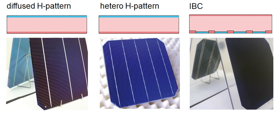
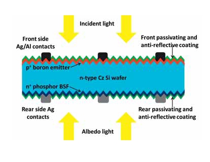
This paper presents recent developments of ECN’s n-Pasha (passivated on all sides H-pattern) solar cell technology. The n-Pasha cell, currently being produced on an industrial scale by Yingli Solar, is a solar cell fabricated on n-type Cz material with homogeneous diffusions, dielectric passivation and printed metallization on both sides. The metallization is applied in an open H-pattern to both sides, which makes it suitable for bifacial applications. In order to improve both cell performance and the cost of ownership of n-Pasha solar cells, the ECN R&D team has focused on several aspects of the device design and processing. By reducing metal coverage and improving the quality of the front-side metallization, tuning the back-surface field (BSF) doping and improving the front- and rear-surface passivation, it has been possible to obtain an average efficiency of 20%, with top efficiencies of 20.2%. At the same time, the amount of silver used for metallization has been decreased by over 50% and is now similar to that used for p-type solar cells. Furthermore, it is shown that with the ECN n-Pasha cell concept, wafers from the full resistivity range of n-Cz ingots can be used to make cells without losses in efficiency. Combining the improved efficiency and the reduction in cost makes the n-Pasha cell concept a very cost effective solution for manufacturing highly efficient solar cells and modules.
Premium
Materials, Photovoltaics International Papers
Module assembly drives as much as a third of the total module cost and can have a significant impact on overall module performance in terms of efficiency and module lifetime. This paper reviews some of the newest moduling material trends, and the outlook for the module market.
Premium
Photovoltaics International Papers, PV Modules
The potential for PV modules to fail before the end of their intended service life increases the perceived risk, and therefore the cost, of funding PV installations. While current IEC and UL certification testing standards for PV modules have helped to reduce the risk of early field (infant mortality) failures, they are a necessary, but not sufficient, part of determining PV module service life. The goal of the PV Durability Initiative is to establish a baseline PV durability assessment programme. PV modules are rated according to their likelihood of performing reliably over their expected service life. Modules are subjected to accelerated stress testing intended to reach the wear-out regime for a given set of environmental conditions. In parallel with the accelerated tests, modules are subjected to long-term outdoor exposure; the correlation between the accelerated tests and actual operation in the field is an ultimate goal of the programme. As understanding of PV module durability grows, the test protocols will be revised as necessary. The regular publication of durability ratings for leading PV modules will enable PV system developers and financiers to make informed deployment decisions.
Premium
Cell Processing, Photovoltaics International Papers
In principle solar cells are very simple: they convert sunlight to electricity and can be characterized by a single number – the solar cell efficiency. Manufacturers obviously want to achieve this efficiency at the lowest possible cost, so it is critical that the efficiency/cost ratio be optimized. To this end, knowledge of where the biggest gains can be achieved is key. This paper presents an in-depth loss analysis method developed at the Solar Energy Research Institute of Singapore (SERIS) and details how various losses in a silicon wafer solar cell can be quantified, which is not done in the case of a conventional solar cell measurement. Through a combination of high-precision measurements, it is shown that it is possible to fully quantify the various loss mechanisms which reduce short-circuit current, open-circuit voltage and fill factor. This extensive quantitative analysis, which is not limited to silicon wafer solar cells, provides solar cell researchers and production line engineers with a ‘health check’ for their solar cells–something that can be used to further improve the efficiency of their devices.

Subscribe to Newsletter

Upcoming Events

Upcoming Webinars
June 30, 2025
10am PST / 6pm BST
Solar Media Events
July 1, 2025
London, UK
Solar Media Events
July 1, 2025
London, UK
Media Partners, Solar Media Events
July 2, 2025
Bangkok, Thailand
Media Partners, Solar Media Events
September 2, 2025
Mexico City, Mexico