
The PV industry is undergoing rapid technology changes that have been driven by the well documented, swift adoption of monocrystalline wafers. Less well understood is that, within this wafer technology transition comes a shift to larger wafer sizes and this includes p-type and n-type mono-Si wafers.
PV Tech has been highlighting for many years that the solar industry was undergoing major technology changes, notably the shift to PERC (Passivated Emitter Rear Cell) and more recently the migration away from multicrystalline wafers to monocrystalline.
Try Premium for just $1
- Full premium access for the first month at only $1
- Converts to an annual rate after 30 days unless cancelled
- Cancel anytime during the trial period
Premium Benefits
- Expert industry analysis and interviews
- Digital access to PV Tech Power journal
- Exclusive event discounts
Or get the full Premium subscription right away
Or continue reading this article for free
These developments have led to the mass production of high-efficiency p-Type mono-PERC, bifacial cells, half-cut and shingled technologies for modules, which are available in double-glass, multi-busbar and half-cell module configurations. All pushing high-efficiency products into the mainstream high-volume markets.
Various n-Type cell options (nPERT and Selective Emitter, for example), as well as heterojunction (HJT) technologies have secured a gradual but increasing foothold in the market, not least because of a shift in wafer size that reduces overall production costs.
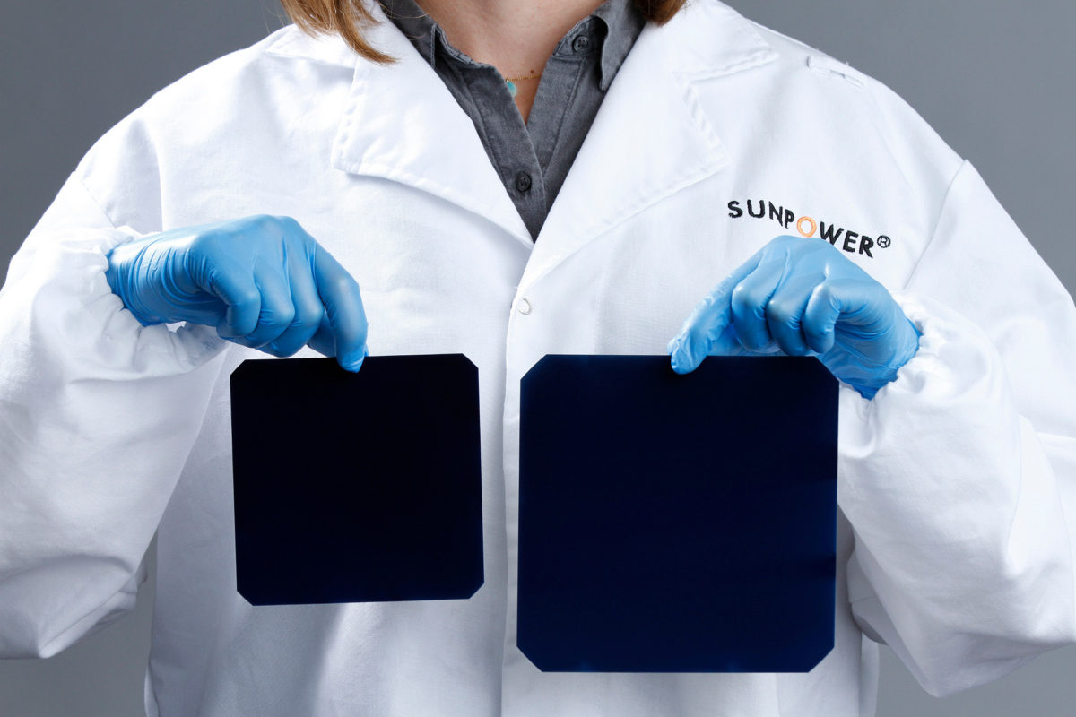
Indeed, a big part of SunPower’s latest NGT (Next Generation Technology) IBC (Interdigitated Back Contact) cell technology, that will power its S-series modules, is the shift to larger n-Type wafers. This is also the path taken by LG Electronics.
Traditionally, monocrystalline silicon wafers before 2010 were classified as small-size with 125mm x 125mm width (164mm silicon ingot diameter) and only a small number at 156mm x 156mm (200mm silicon ingot diameter), which had been the dominant ingot size in the semiconductor industry until leading companies adopted 300mm diameter ingots.
Monsoon Wang, Director of Product Marketing at LONGi Solar told PV Tech that the wafer size change is occurring faster than many people realise.
“Yes, this trend is happening,” noted Wang. “Only ten years ago, almost all the mono wafers were 125mm. A few years later some producers were starting to supply 156mm wafers and we have seen that these almost complete transitions can take two to three years. So by 2014, the transition to 156mm wafers had happened. The reason for this change is that the wafers were much smaller and production costs much higher as the overall capacity was much lower than for multi. This was the driver for all cell producers to switch to the then larger wafer size.”
After 2010, 156mm x 156mm wafers increasingly became the popular choice (lower cost per-watt) for p-Type mono and multi wafer sizes. As a result of the lower production costs, 125mm x 125mm P-type wafers were almost eliminated from the market by 2014, with only some IBC and HJT cells using the 125mm x 125mm n-Type wafers as the larger size technology lagged P-type investments due to the niche nature of the applications.
By the end of 2013, a number of China-based wafer producers (LONGi, Zhonghuan, Jinglong, Solargiga and Comtec) jointly issued the standards for (M2) 156.75 x 156.75 p-Type mono wafers (205mm diameter silicon ingot) and (M2) 156.75 x 156.75 p-Type mono wafers (210mm diameter silicon ingot).
Without increasing the overall dimensions of a 60-cell module, M2 wafers could increase module power by more than 5Wp, a significant boost for a competitive cost per-watt, thus rapidly becoming the mainstream and maintaining that status for several years.
During that period, there were also a few (M4) 161.7mm x 161.6mm (211mm diameter silicon ingot) wafers on the market, the area of which was 5.7% larger than an M2, and these were mainly used for n-Type bifacial modules.
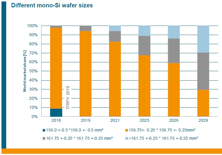
The move from 156mm x 156mm to the larger formats of 156.75mm x 156.75mm in mass production started in 2016. The old 6” format (156mm x 156mm) we all recognise is expected to disappear completely from the market by the end of 2019, according to the 2019 edition of the ITRPV survey.
However, a transition to a new larger ‘standard’ wafer size is going to prove difficult, as will comparing cell/module conversion efficiencies on a like for like basis going forward.
The industry is transitioning faster than expected and key PV module manufacturers such as LONGi and JinkoSolar are ramping mono-Si wafer capacity, which is compatible with the production of larger silicon wafers. Multicrystalline wafer sizes are also expected to follow suit. The dominant format is 156.75 x 156.75 in mass production but, according to the ITRPV 2019 edition, other sizes are also emerging in mass production, such as 157 x 157 and even a larger format at 158.75 x 158.75, could be the standard for the next few years.
Larger formats are expected to enter production at some point, including 166mm x 166mm, which could gain a 15% market share over the next 10 years. Even larger formats are not ruled out in the latest ITRPV survey.
This is more than likely due to intensified market competition seen in the second-half of 2018, when China cut support mechanisms for utility-scale and Distributed Generation markets under the ‘531 New Deal.’
“During the second-half of last year [2018], due to market requirements customers were asking for higher module outputs in the 400Wp range,” added Wang. “This is very difficult to achieve at the cell level in such a short time. Changing the wafer size and moving to half-cut cells was seen as the best option to get to 400Wp.
However, several manufacturers had their own ideas on what the larger wafer size should be, such as 157.4mm, 158.75mm and 161.7mm, which Korean firms such as LG and Q CELLS selected for n-type wafer cells. So in the second-half of last year there was some uncertainty in the market, which led to discussions with a lot of customers. What we found was the key concern centred around the impact on the LCOE of PV projects.
The [downstream] market will need time to be informed and educated about the next wafer transition, especially in module dimensions and weight comparisons with say glass/glass bifacial modules. A key point to consider when moving to slightly larger module dimensions is that the modules will still only need two people to install, so the LCOE will still be lower, as will the BOS (Balance of System).
This also applies to cell manufacturing, with cost per-watt also reduced, along with paste. Although it could be a little difficult for existing cell and module production capacity to adopt the larger wafer sizes, as capex would need to be spent on certain upgrades, new production lines would not have that difficulty,” added Wang.
The thought process at play was the hope that a further increase of module power outputs by expanding the size of silicon wafers would be the cheapest route to secure product competitiveness.
According to LONGi, one route that PV manufacturers had evaluated was to adopt M2 wafers and continue to increase the width across the wafer, to 157mm, 157.25mm or 157.4mm, without increasing the overall dimensions of the module.
However, modelling indicated that the increase in power output would be limited. Other factors, such as requirements on production accuracy, would also be increased. Furthermore, the certification compatibility could be affected (e.g. failing to meet the creepage distance requirement of UL certification).
LONGi noted that another methodology was to follow the route of increasing the width across the wafer from 125mm to 156mm, increasing the size of the module, such as 158.75mm pseudo-square wafer or square wafer (223mm diameter silicon ingot). LONGi stated that the latter increases the wafer area by about 3%, which in turn increases the power of a 60-cell module by nearly 10Wp.
What also seems to be happening is that n-Type module manufacturers could be choosing 161.7mm M4 wafers, while some plan to launch 166mm sized wafers in the future, according to LONGi.
Perhaps not surprising is that the largest mono wafer producer has chosen the 166mm wafer size, as this is apparently the maximum size compatible with all standard horizontal diffusion furnace production tools. On the one hand, the depreciation and manual labour per watt will be significantly reduced due to the increase of the production capacity for cells and modules. On the other hand, modules with larger wafers have higher power and can reduce BOS cost, which in turn will reduce the total cost of the system.
With larger wafers, the need for half-cut or multi-cut cells also increases, due to the increase in negative resistive losses for p-Type mono-based cells. Less resistance between the cells clearly increases the power output of a module.
So, going forward, for p-Type mono-based cells, bigger is going to be better, as long as cut cells and other cell-to-module loss reduction technologies, such as shingling, are adopted.
“There is a growing consensus amongst manufacturers that the next standard will be the 166mm size M6 wafer, after we publicly launched it at SNEC. There will be work undertaken to informl the market about this next standard wafer as, being the number one mono wafer producer, we have that responsibility.
From LONGi’s perspective it will take around half a year to make the transition to the M6 wafer in a module and perhaps a year for the industry to transition to the M6 wafer. There is a good incentive to transition as quickly as possible,” concluded Wang.

")


