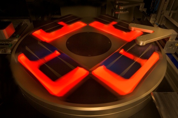
There is no more doubt that PERC is becoming a mainstream technology in standard industrial solar cell production. The question arising is “what is next?”
A good candidate to make the race to become a new standard process is Cu metallisation to replace the costly Ag printing, which accounts for almost 50% of the solar cell production cost.
Try Premium for just $1
- Full premium access for the first month at only $1
- Converts to an annual rate after 30 days unless cancelled
- Cancel anytime during the trial period
Premium Benefits
- Expert industry analysis and interviews
- Digital access to PV Tech Power journal
- Exclusive event discounts
Or get the full Premium subscription right away
Or continue reading this article for free
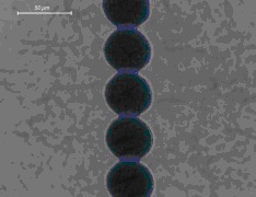
Select companies have teamed to developed an electroplating process to directly deposit a stack of Ni, Cu, and Ag on laser opened areas of the Si substrate (Plating on Silicon, PoSi). The technology package comprises of a front-side LCO process followed by subsequent PoSi and post annealing processes, which can be directly integrated into existing production lines as an upgrade.
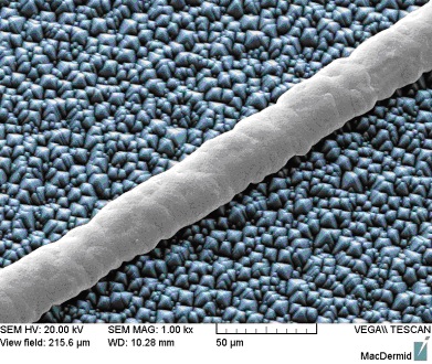
As a result, a proven industrial solution is being offered for the first time where the formerly well known adhesion problems of the metal stack after soldering have been solved. The key to this technology is the choice of the right laser process together with a perfect adaption of the plating method and chemistry.
In contrast to the rear side LCO process for PERC, the front-side LCO process for PoSi does not allow any melting of the textured Si surface and damage to the sensitive junction, while the passivation layer must be removed thoroughly with no residues hindering the onset of the metal growth process. The technology developed by RENA, MacDermid, and InnoLas works for standard as well as PERC solar cells and does not require any changes to the standard module assembly and soldering process. Module reliability tests have already been passed successfully with excellent results and no degradation of the module performance after heat cycling testing.
Laser fired contacts (LFC) are commonly seen as next-generation PERC technology, whereby the Al printing and co-firing steps are substituted by a layup of an Al foil directly onto the passivated rear side, which is locally fired and subsequently cut out by lasers, all being processed within one single piece of laser equipment. This will enable a significant cost reduction compared to the actual LCO, Al printing and co-firing processes. Partnering with the patent owning technology developer Fraunhofer ISE, InnoLas has already developed the required laser processes as well as prototype equipment for the foil layup. Challenges still to be solved are on the industrial maturity of the technology and passing the module reliability testing.
IBC or IBC-related solar cell concepts are starting to become more and more relevant for companies, who managed to exceed a certain level of cell efficiency performance. IBC cell architecture represents a more significant step in the efficiency roadmap than evolutionary steps like PERC, PoSi, or n-type bifacial cells.
There is a significant gap between the requirements of, for example, a standard production line with PERC upgrade and a fully blown IBC production line in terms of process stability, reliability and precision, and the equipment for IBC production must fulfill specifications close to semiconductor standards.
For example, an alignment accuracy of down to ±10 µm with an absolute precision of ± 5 µm in 24/7 production must be achieved. The complete control of all functions of a leading-edge ultra-short pulse laser source is only one of the required enhanced features next to an integrated analytics for inline characterisation of the laser process result to close the feedback loop with the machine and to assure that the process result is always within a tight process window.
The most obvious application for laser processes on IBC cell architectures is again an LCO process substituting the cost-intensive photo-lithography and wet etching processes, which were needed to create the metal pattern of the interdigitated fingers. Besides LCO, there are a couple of other possible applications for laser processing on IBC, which are still under investigation.
Requirements on laser machines for mass production
In simple terms a laser machine includes a laser source, a scanner, some optical components and a controlled x/y stage, components that are technically available off the shelf, giving the impression that a production tool could be built by anyone.
This fundamental misunderstanding often led to frustration and jeopardised the success of laser machines as a highly cost effective and even enabling technology in the PV industry. A variety of unavoidable influencing factors from outside, such as temperature variations, vibrations and pollution, amongst others, lead to degradation of the laser beam quality and alignment, which must be eliminated by proper countermeasures in the machine design.
Insufficient exhaust causes a so-called clouding effect, which is a cloud of dust generated from removed material during a laser ablation process. Laser sources naturally exhibit a certain level of power degradation over time, which must also be compensated for.
This had led to a number of key additional technologies for laser tools to meet volume production requirements such as high-speed galvanometer scanners, automatic vision alignment and machine calibration systems to assure a very high accuracy and stability in a 24/7 production environment as well as extremely high throughputs of up to 3,600 wafers per hour for various process applications.
Other than wet chemical, CVD or printing processes, laser processing is almost free from consumable costs. Main contributors to cost of ownership are capital investment per throughput, maintenance cost and operating cost. Therefore the task of the laser equipment provider is to design a system that is based on a standardised and proven industrial platform.
A few examples of this include the use of nanosecond laser sources, which are cheaper than picosecond laser sources and can be superior in performance for LCO through their ability to create a melting zone at the Si surface. They can achieve the highest throughput through very high repetition rates and can provide enough power for supplying two process heads with one laser source, presuming the right laser source is chosen by the machine vendor.
Maintenance and spare part costs can be minimised by choosing a laser source with a diode lifetime greater than 40,000 hours and with no need for an external cooling system. Stationary processing with conventional scanner technology is by far more reliable and cost effective than so-called on-the-fly processing with polygon scanners. System uptime can be optimised by automatic calibration routines, which avoid stopping the production machine for mechanical adjustments.
Conclusion
The historical role of laser processing for the fabrication of industrial standard c-Si solar cells is ambiguous. Several applications for lasers such as via drilling, laser edge isolation and laser doped selective emitters emerged and vanished. Laser contact opening is about to establish itself as a mainstream technology in the PV industry and is indispensable for PERC solar cells.
State-of-the-art laser machines for mass production must dispose of automatic routines to compensate for misalignments and laser degradations over time, and must be able to run sophisticated patterns at a very high speed and throughput in order to achieve optimum efficiency at affordable cost. In future, the laser contact opening will play an increasingly important role, for example for electroplated Cu metallization or IBC solar cells.
Current and future trends in c-Si cell manufacturing will be the focus of the inaugural PV CellTech conference to be held in Kuala Lumpur, Malaysia, on 16-17 March 2016. Organised by PV Tech's publisher Solar Media, the event will feature presentations from leading figures from the world of silicon solar manufacturing and R&D. Further details are available here.
Authors
Ernst Hartmannsgruber received a diploma in physics in 1995 from the Technische Universität Berlin, Germany. Already as a student he was engaged by the Fraunhofer Society, where he worked for 10 years in R&D for advanced semiconductor technology. In 1999 he became a sales manager for production equipment in the semiconductor industry. Meanwhile his background includes 16 years of sales experience in the semiconductor and photovoltaic industries at several market leading equipment suppliers. In 2014 Ernst Hartmannsgruber joined InnoLas Solutions as director of sales and marketing.
Dr. Rico Böhme received his PhD in engineering sciences from the Martin Luther University, Halle-Wittenberg in 2007. After he had worked for seven years as scientific employee at several institutes for laser technology, he became a senior engineer for laser and metallisation processes and a member of the PV turnkey team at the R&D department of Roth & Rau AG in 2008. In 2011 Böhme joined InnoLas, where he was project manager & head of process development and since 2014 he has been the business development manager of the InnoLas Solutions.
The first part of this guest blog can be viewed here.
Dr. Rico Böhme and Ernst Hartmannsgruber represent laser tool systems manufacturer InnoLas Solutions GmbH.
PV Tech and Solar Intelligence plan to present the most comprehensive and in-depth analysis of the latest manufacturing capacity expansion developments at the inaugural PV CellTech technical conference being held in Kuala Lumpur, Malaysia between 16 – 17 March, 2016. More details on how to attend can be viewed here.


