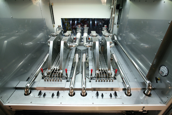
Schmid`s APCVD (Atmospheric Pressure Chemical Vapor Deposition) technology allows for a variety of doped and undoped films to be deposited inline that can boost solar cell conversion efficiencies for a wide range of solar cell architectures for high-volume production such as PERC and PERT.
Problem
Try Premium for just $1
- Full premium access for the first month at only $1
- Converts to an annual rate after 30 days unless cancelled
- Cancel anytime during the trial period
Premium Benefits
- Expert industry analysis and interviews
- Digital access to PV Tech Power journal
- Exclusive event discounts
Or get the full Premium subscription right away
Or continue reading this article for free
Higher efficiency cell architectures are required to meet LCOE cost reduction requirements across residential, commercial and utility-scale PV markets globally. However, factors such as PID (Potential Induced Degradation and LID (Light Induced Degradation) hamper the realization of performance advances. One of the main drivers to adopt N-type solar cells regards LID, which occurs in p-type silicon after being exposed to light leading to a permanent 0.5-1% drop in cell efficiency. Doping n-type silicon with boron can also be done using either ion implantation or thermal diffusion using boron precursors. However, when introduced inside the tube, the boron depletes resulting in poor uniformity across the wafers. Moreover, precursor byproducts leave a residue which can cause both the wafer carrier and wafers themselves to stick, leading to more costly maintenance and downtime. In addition, thermal diffusion using precursor injection into the tube leads to doping both surfaces of the wafer unless additional masking steps are applied. Lastly, the process leaves a boron oxygen rich layer on the cell surface which must be removed requiring further thermal and wet chemistry steps, hindering throughput and operation costs.
Solution
SCHMID`s APCVD technology allows for a variety of doped and undoped films to be deposited inline. The APCVD can deposit undoped silicon glass (USG), phosphorus silicate glass (PSG), boron silicate glass (BSG), and titanium oxide (TiO2). Film thickness and dopant concentrations can be adjusted to fit a variety of cell designs.
In the case of n-type cells, a BSG layer can be deposited inline, with desired thickness and concentration, capable of achieving excellent uniformities to form a high performance p-n junction after drive-in.
Applications
APCVD has been used for creating high efficiency boron doped N-type cells, IBC cells, back junction, and bifacial cell architectures.
Platform
SCHMID`s APCVD systems are offered in belt or roller variants. They can be configured for multiple films and film stacks in a single pass. Film thickness can reach up to 200nm with finely controlled dopant concentration and uniformity.
Availability
Currently available.


