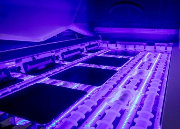
Applied Materials has entered the solar wafer inspection market with ‘Applied Vericell’ system designed to fully-automate in-line wafer inspection to address the quality limitations of manual review, with the capability to automatically predict wafer cell efficiency through photoluminescence (PL) technology. The Vericell system is being introduced at SNEC 2014 in Shanghai, China.
Problem
Declining ASPs make cost of ownership (CoO) reduction & production yield critical items for every solar wafer and cell manufacturer, while keeping costs low while maintaining R&D expenditures. Wafer manufacturers must deliver high quality wafers at a competitive price to cell producers which in-turn must produce high efficiency cells in volume while maintaining high production yields. Being able to cost-effectively track all incoming and outgoing wafer quality and adjust manufacturing processes to improve yield and binning to remove low-efficiency wafers and identifying those that require process modifications provides the potential for significant cost savings.
Try Premium for just $1
- Full premium access for the first month at only $1
- Converts to an annual rate after 30 days unless cancelled
- Cancel anytime during the trial period
Premium Benefits
- Expert industry analysis and interviews
- Digital access to PV Tech Power journal
- Exclusive event discounts
Or get the full Premium subscription right away
Or continue reading this article for free
Solution
The Vericell system’s multiple integrated inspection modules automatically evaluate each wafer to find and eliminate defective wafers from production. It measures and reports on a range of parameters including wafer thickness, thickness variations, warp and resistivity. The system also detects defects including saw marks, chipped edges, stains, and micro-cracks. By controlling quality and minimizing the risk and costs of wafer breakage from manual inspection, the Vericell tool provides the opportunity for significant gain in factory production. Employing photoluminescence (PL) technology combined with multiple sensing capability and advanced software algorithms, the Vericell system can predict final cell efficiency from bare wafer material with a mean average prediction error of less than 0.15% on multi-crystalline silicon wafers, according to the company. Removing low-efficiency wafers and identifying those that require process modifications provides overall improvement in a factory’s output of higher efficiency cells, which can significantly improve profitability. While PL technology has been used for inspection, the automation capabilities of the Vericell tool enable its predictive accuracy and easy integration into existing production lines.
Applications
c-Si wafer inspection and predictive final solar cell efficiency mapping.
Platform
The Vericell system is available with Applied’s proprietary yield management software that can be utilized to collect, consolidate and analyze real-time data. This software allows customers to quickly identify and act on yield-impacting events to optimize their entire manufacturing line. The Plug and play architecture supports customization and easy module expansion to include higher levels of inspection.
Availability
May 2014 onwards.

