Cell Processing

Premium
Cell Processing, Photovoltaics International Papers
Since the first demonstration by Sanyo in the 90s of crystalline silicon heterojunction (SHJ) solar cells with already promising energy conversion efficiencies above 18%, this device architecture has experienced an extraordinary history of development, embodying outstanding scientific findings and efficiency records.
Premium
Cell Processing, Photovoltaics International Papers
During 2017, the PV industry is forecast to produce and ship close to 100GW of solar modules, reaching this key milestone well ahead of all market forecasts previously projected. Furthermore, the explosive growth of solar PV shows no sign of abating, despite the constant threats and barriers imposed by on-going trade import restrictions.
Premium
Cell Processing, Photovoltaics International Papers
Modern single metallization lines using flatbed screen printing (FSP) can realize a maximum output of approximately 2,000 wafers/h. For several reasons, achieving a significant further increase in throughput of the FSP process is technically challenging.
Premium
Cell Processing, Photovoltaics International Papers
The first appearance of a shingled solar cell interconnection pattern (see Fig. 1) dates back to 1956 with a US patent filed by Dickson [1] for Hoffman Electronics Corporation, which is just two years after the first publication of a silicon solar cell by Chapin et al. [2]. In the years that followed, further patents were filed containing concepts of shingling solar cells serving various module designs and applications – for example, Nielsen [3] for Nokia Bell Labs, Myer [4] for Hughes Aircraft Company, Baron [5] for Trw Inc, Gochermann and Soll [6] for Daimler-Benz Aerospace AG, Yang et al.
Premium
Cell Processing, Photovoltaics International Papers
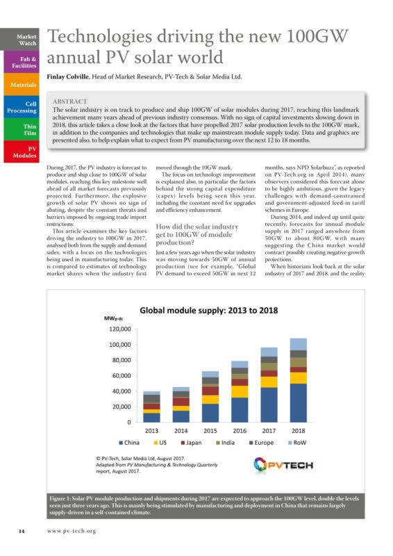
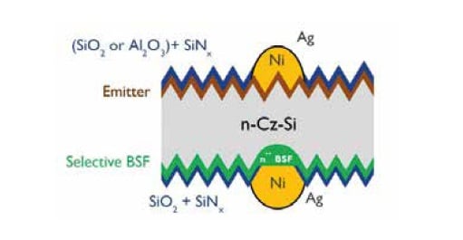
For many applications, bifacial modules offer a cost-effective way of increasing energy yields, which explains why the interest in bifacial cells in the PV industry is steadily growing and is expected to continue. However, the metallization of bifacial cells creates new challenges, as the same materials and techniques developed for n surfaces are generally not directly, or simultaneously, applicable to p surfaces; this necessitates sequential metallization of each side, resulting in added cost and/or complexity. This paper introduces a simple co-plating approach with the objective of simplifying the metallization of bifacial cells in a cost-effective way, and which is designed for multi-wire module integration. The metallization route is described, and high cell efficiencies of up to 22.4% are demonstrated using this co-plating approach with bifacial nPERT+ cells (where ‘+’ signifies the bifacial nature of these cells). Initial thermal-cycling reliability data of test structures and 1-cell laminates is presented. Finally, cost-of-ownership (COO) estimates are given, which predict the co-plating approach to be ~40% cheaper than bifacial screen-printed metallization. It is shown that the combination of the high efficiency potential of nPERT+ cells and the reduced costs of co-plating has the potential to deliver module-level costs of ~$0.25/Wpe (glass–glass configuration).
Premium
Cell Processing, Photovoltaics International Papers
There are numerous tools and methods available on the market for the optical and electrical quality control of high-efficiency silicon solar cells during their industrial production, and even more are discussed in the literature. This paper presents a critical review of the possibilities and limitations of these tools along the value chain, from wafer to cell, in the case of passivated emitter and rear cells, as well as a discussion of some showcases. Economic and technological challenges and future trends are addressed.
Premium
Cell Processing, Photovoltaics International Papers
A novel nanoscale pseudo-pit texture has been formed on the surface of a multicrystalline silicon (mc-Si) wafer by using a metal-catalysed chemical etching (MCCE) technique and an additional chemical treatment. A desirable nanoscale inverted-pyramid texture was created by optimizing the recipe of the MCCE solution and using a proprietary in-house chemical post-treatment; the depth and width of the inverted pyramid was adjustable within a 100–900nm range. MCCE black mc-Si solar cells with an average efficiency of 18.90% have been fabricated on CSI’s industrial production line, equating to an efficiency gain of ~0.4%abs. at the cell level. A maximum cell efficiency of 19.31% was achieved.
Premium
Cell Processing, Photovoltaics International Papers
This paper presents an in-depth analysis of state-of-the-art p-type monocrystalline Czochralski-grown silicon passivated emitter and rear cells (PERCs) fabricated in a near-industrial manner. PERC solar cells feature a homogeneous emitter on the front side, and an Al2O3 passivation layer and local contacts on the rear side.
Premium
Cell Processing, Photovoltaics International Papers
A highly promising concept for future solar cells is the heterojunction (HJT) architecture; according to the ITRPV roadmap 2016, the market share for HJT solar cells will increase to 10% by 2026. Over this timescale, stabilized cell efficiency will increase to 24%, which is the second-highest predicted efficiency after backcontact cells with n-type mono-Si. Moreover, metallization of HJT cells offers the advantage of using low-temperature steps, which reduces energy consumption and hence production costs.
Premium
Cell Processing, Photovoltaics International Papers
This paper presents the fabrication of front-junction n-type silicon solar cells with Cu-plated electrodes, using laser contact opening and forward-bias plating. The cells feature a back-surface field formed by a phosphorus implant, and a diffused boron emitter with aluminium oxide passivation. Laser ablation of the front-side dielectric layers is followed by a metallization based on Ni/Cu forward-bias plating, while sintered metal paste is used for the rear electrode. The results show improved line conductivity and contact resistivity for the plated electrode, leading to higher solar cell efficiency than for cells made with conventional Ag/Al paste. On 6" n-type Czochralski wafers, cell efficiencies of up to 21.3% have been demonstrated, with an open-circuit voltage of 654mV, a short-circuit current of 40.8mA/cm2 and a fill factor of 79.8%.

Subscribe to Newsletter

Upcoming Events

Solar Media Events
May 21, 2024
Sydney, Australia
Solar Media Events
May 21, 2024
Napa, USA
Solar Media Events
May 22, 2024
London, UK
Upcoming Webinars
May 29, 2024
11am (EDT) / 5pm (CEST)