Photovoltaics International Papers

Premium
Cell Processing, Photovoltaics International Papers
This paper presents the background and technology development of the use of ion implantation technology in today’s crystalline silicon solar cell manufacturing lines. The recent history of ion implantation development and commercialization is summarized, and an explanation is given for the cell efficiency improvements realized using the technique on p-type mono-crystalline cells. The potential economic impact on the factory is also discussed.
Premium
Cell Processing, Photovoltaics International Papers
Reducing the cost of photovoltaic energy is the main objective of solar cell manufacturers. This is ideally realized by increasing cell efficiency and simultaneously decreasing manufacturing cost. To reduce fabrication costs, the international roadmap of photovoltaics (ITRPV) forecasts a reduction in cell thickness from 180μm to 120μm in the next six years, and even thinner cells may be desirable, as long as efficiency and yield are not negatively affected. In order to increase efficiency, the ITRPV forecasts an increase in share of back-contacted cells from 5% to 35% in the next eight years. In this paper the dependence of the efficiency of back-junction back-contact (BJBC) solar cells on cell thickness is investigated experimentally and numerically. To this end, BJBC silicon solar cells with cell thicknesses ranging from 45μm to 290μm are fabricated and simulated. Thinned float-zone material is used as well as monocrystalline epitaxial layers fabricated by the porous silicon process for 45μm-thick cells. The efficiency of the best cell is 22.6% (130μm cell thickness) and 18.9% for an epitaxial cell (45μm thickness). Loss mechanisms in the maximum power point of all cells are investigated by using a freeenergy loss analysis based on finite-element simulations. A lower generation and a lower recombination in thinner cells compete against each other, resulting in a maximum efficiency of 20% for a cell thickness of 45μm at a base lifetime of 20μs. At a base lifetime of 3000μs, the maximum efficiency is greater than 23% for a cell thickness beyond 290μm, but reducing the cell thickness from 290μm to about 90μm results in a power loss of less than 0.6% absolute.
Premium
Cell Processing, Photovoltaics International Papers
The market price of Ag has fluctuated considerably over the past ten years and has impacted the manufacturing cost of Si solar cells and the price of Si PV. Reducing Ag consumption can decrease this cost; however, such reduction may come at the expense of cell performance. In order to address the issue of Ag cost reduction while maintaining high cell efficiency, phosphorus emitter profiles are tailored via POCl3 diffusion to create solar cell emitters displaying low saturation current density (J0e), variable electrically active surface phosphorus concentration ([Psurface]), and variable sheet resistance with the aim of reducing Ag consumption. By optimizing emitter diffusion conditions, it is possible to reduce screen-printed Ag paste consumption by 33% with no loss in cell performance. Using a screen-printable Ag conductor paste designed to contact low [Psurface] emitters, the performance of cells with screen-printed Ag paste dry masses of 200, 120 and 80mg is compared. By using a tailored low-J0e 55Ω/sq emitter, it is possible to achieve a high open-circuit voltage (Voc) and short-circuit current (Jsc) to yield average cell efficiencies of 18.64% and 18.73% for 120mg and 80mg Ag paste dry mass, respectively. This is compared with efficiencies of 18.52% for cells using state-of-the-art technology (industrial high [Psurface] 65Ω/sq emitter with 120mg Ag paste dry mass). On the basis of a Ag market price of US$32/troy oz and an 85% by weight thick-film paste Ag metal content, a Ag front-side metallization cost of US¢2.11/W can be achieved by using 80mg Ag paste dry mass, which translates to a Ag cost saving of US$5.4M per year for a 500MW production line when compared with the Ag cost for state-of-the-art technology. Further cost analysis shows a 1.2% area-related balance of system (BOS) cost reduction and a US¢0.1/kWh reduction when comparing low-J0e 55Ω/sq modules and state-of-the-art modules. Calculations show that an additional 0.5% absolute efficiency for state-of-the-art modules is required, to compensate the efficiency gains and Ag cost reduction afforded by low-J0e 55Ω/sq modules.
Premium
Materials, Photovoltaics International Papers
A record-low spot price in the wake of oversupply and the aggressive cost-reduction roadmap of the PV industry are putting polysilicon producers under pressure to bring down their manufacturing costs. With the dominant Siemens process approaching a limit for further cost cuts, technologies based on the deposition from monosilane (SiH4) have now become the focus of attention.
Premium
Materials, Photovoltaics International Papers
The cost of PV modules manufactured and sold in 2012 is highly reliant on the materials used in the construction. A significant part of the market price is driven by the bill of materials, while other direct costs and depreciation form a small proportion of the total cost. Changes within the supply chain, and in the cost of the materials needed and used, are extremely important influences on the module cost and the end market price. In 2012 we have seen a slowdown in growth in the installation of both commercial and residential PV, despite dramatic falls in module costs. Some of the trends and effects of these changes on the materials supply chain for PV modules will be examined in this paper.
Premium
Fab & Facilities, Photovoltaics International Papers
Production equipment is the backbone of the PV industry, but the equipment sector is suffering because of overcapacity. The 2012 global capacity utilization is at 55% for crystalline silicon (x-Si) module production, 70% for cadmium telluride (CdTe) and 80% for copper indium gallium (di)selenide (CIGS). Under these market conditions, there are almost no expected capacity expansions in the near term. The overcapacity has driven the average selling price (ASP) for modules significantly lower, resulting in hyper-competition in the PV industry, where almost all PV companies recognize the importance of product differentiation while still reducing costs. These market conditions present an opportunity for equipment manufacturers to differentiate their offerings through enabling lower production costs and higher efficiency of cells and modules.
Premium
Photovoltaics International Papers, PV Modules
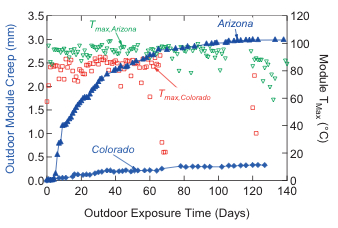
There has been recent interest in the use of thermoplastic encapsulant materials in photovoltaic modules to replace chemically cross-linked materials, for example ethylene-vinyl acetate. The related motivations include the desire to reduce lamination time or temperature, to use less moisture-permeable materials, and to use materials with better corrosion characteristics or improved electrical resistance. However, the use of any thermoplastic material in a hightemperature environment raises safety and performance concerns, as the standardized tests do not currently include exposure of the modules to temperatures in excess of 85°C, even though fielded modules may experience temperatures above 100°C. Eight pairs of crystalline silicon modules and eight pairs of glass/encapsulation/glass thin-film mock modules were constructed using different encapsulant materials, of which only two were designed to chemically cross-link. One module set with insulation on the back side was exposed outdoors in Arizona in the summer, and an identical set was exposed in environmental chambers. High-precision creep measurements (±20μm) and performance measurements indicated that, despite many of these polymeric materials being in the melt state during outdoor deployment, there was very little creep because of the high viscosity of the materials, the temperature heterogeneity across the modules, and the formation of chemical cross-links in many of the encapsulants as they aged. In the case of the crystalline silicon modules, the physical restraint of the backsheet reduced the creep further.
Premium
Photovoltaics International Papers, PV Modules
Apart from aesthetics, the gain in electrical performance of back-contact solar cells and modules is particularly attractive compared to conventional PV modules. This major benefit results from getting rid of (the majority of ) the metallization at the front, and providing all the cell contacts at the back. An overview is presented here of the different concepts put forward by different institutes and companies around the world for such back-contact modules. The different types of state-of-the-art back-contact cell are first introduced, together with their corresponding contacting and interconnection schemes. Keeping in mind the reference module technology for two-side-contacted cells as a starting point, each module concept is then briefly discussed in terms of technology and level of maturity. Finally, the main technological differences are summarized.
Premium
Photovoltaics International Papers, Thin Film
Thin-film PV modules are one of the most sustainable options for the generation of electricity, with low material consumption and short energy-payback times. Both of these factors are essential for paving the way towards a terawatt PV market. However, the cost-competitive production of PV modules has become extremely difficult, and module producers are facing huge challenges. A rapid technology transfer from research to industry is therefore required in order to introduce innovations for lower production costs and higher conversion efficiencies. At the Competence Centre Thin-Film- and Nanotechnology for Photovoltaics Berlin (PVcomB), founded by the Helmholtz-Zentrum Berlin (HZB) and the Technical University Berlin, two R&D lines for 30 x 30cm2 modules based on thin-film silicon and copper indium gallium (di)selenide (CIGS) respectively are operated. Robust baseline processes on a high efficiency level, combined with advanced process and device analytics, have been established as a basis for the introduction and development of further innovative technology steps, and their transfer to industry.
Premium
Photovoltaics International Papers, Thin Film
Thin-film solar cells (TFSCs) still hold unlocked potential for achieving both high efficiency and low manufacturing costs. The formation of integrated interconnects is a useful way of maintaining high efficiency in small-scale solar cells by their connection in series to form a module. Laser scribing is widely used for scribing a-Si- and CdTe-based TFSCs to form interconnects. The optical properties of the ternary copper-indium-gallium (di)selenide (CIGS) compound are well suited to the solar spectrum, with the potential to achieve a high photoelectrical efficiency. However, since it is a thermally sensitive material, new approaches for the laser-scribing process are required, to eliminate any remaining heating effects. For flexible CIGS solar cells on non-transparent substrates (metal foils or polymer), the scribing process faces additional challenges. This is one reason why ultrashort laser pulses yield better results in terms of scribing quality and selectivity. The modelling of laser energy coupling and an extensive characterization of laser scribes allow approaches to be developed for laser scribing of CIGS solar cells on flexible polymer substrates. The measured high efficiency of the resulting high-speed laser-scribed, integrated CIGS mini-modules proved the capability of this approach.

Upcoming Events

Solar Media Events
February 3, 2026
London, UK
Upcoming Webinars
February 18, 2026
9am PST / 5pm GMT
Solar Media Events
March 24, 2026
Dallas, Texas
Solar Media Events
April 15, 2026
Milan, Italy
Solar Media Events
June 16, 2026
Napa, USA