By Amine Mansouri, Researcher, GE Global Research Europe; Martin Bucher, Researcher, GE Global Research Europe; Frederick Koch, Master's Student, GE Global Research Europe; Marcus Zettl, Solar Lab Leader, GE Global Research Europe; Mark Lynass, Head Scientist in Solar, GE Global Research Europe; Oleg Sulima, Senior Photovoltaic Scientist, GE Global Research; Oliver Mayer, Principal Scientist in Solar Systems, GE Global Research Europe; Omar Stern, Senior Scientist in Solar Technologies, GE Global Research Europe
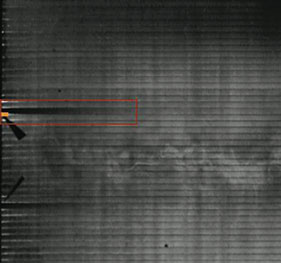
Electroluminescence (EL) imaging for photovoltaic applications has been widely discussed over the last few years. This paper presents the results of a thorough evaluation of this technique in regard to defect detection in photovoltaic modules, as well as for quality assessment. The ability of an EL system to detect failures and deficiencies in both crystalline Si and thin-film PV modules (CdTe and CIGS) is thoroughly analyzed, and a comprehensive catalogue of defects is established.
For crystalline silicon devices, cell breakages resulting from micro-cracks were shown to pose the main problem and to significantly affect the module performance. A linear correlation between the size of the breakages and the power drop in the module was established. Moreover, mechanical stress and temperature change were identified as the major causes of the proliferation of cracks and breakages. For thin-film modules, EL imaging proved the existence of an impressive reduction in the size of localized shunts under the effect of light-soaking (together with a performance improvement of up to 8%). Aside from that, the system voltage was applied in order to monitor transparent conductive oxide (TCO) corrosion effects and laser-scribing-induced failures, as well as several problems related to the module junction box in respect of its sealing and the quality of its electric connectors.