Photovoltaics International Papers

Premium
Photovoltaics International Papers, PV Modules
Solar enterprises will each be faced with the occasional surplus or lack of solar modules in their lifetimes. In these instances, it is useful to adjust these stock levels at short notice, thus creating a spot market. Spot markets serve the short-term trade of different products, where the seller is able to permanently or temporarily offset surplus, while buyers are able to access attractive offers on surplus stocks and supplement existing supply arrangements as a last resort.
Premium
Photovoltaics International Papers, PV Modules
This paper, the fourth in a series covering cost modelling studies for photovoltaics [1–3], examines a new approach to module assembly based on the concept of ‘supersized’ 1kW PV modules. Using supersized modules (1.6m × 3.8m) and integrated microinverters, this novel approach has the estimated potential to save utility solar installations nearly $0.50/Watt. The paper will conclude with a detailed cost and resource case study comparing two 40MW module lines, one employing ‘solar breeder’ technology and the other producing conventional-sized modules.
Premium
Photovoltaics International Papers, PV Modules
This paper presents fluorescence detection as a new tool for the investigation of the degradation of EVA. The superior sensitivity of the set-up contained herein allows an early assessment of the changes of the EVA after only 20 hours of damp-heat exposure. A newly developed scanning system allows the spatially resolved inspection of entire PV modules. Degradation of the encapsulants was detectable after two years’ outdoor exposure, as was the effect of cracks in c-Si cells, which coincide well with cracks made visible by electroluminescence.
Premium
Photovoltaics International Papers, Thin Film
The three most viable thin-film photovoltaic technologies – cadmium telluride (CdTe), copper-indium gallium (di)selenide (CIGS), and amorphous silicon (a-Si) – continue to mature and grow technologically and in market stature. But apart from the dominance shown by CdTe leader First Solar, the rest of the TFPV manufacturers have had a fairly difficult time making significant commercial inroads as the price of mainstream crystalline-silicon modules plummeted over the past couple of years. Other factors delaying the long-predicted age of thin film include bankability challenges and difficulties in reducing production and system costs. Yet entrants in all three thin-film categories have reason for optimism, as they push toward a competitive market position. This paper provides an overview of the current status of the thin-film PV sector and its players, offering insights into why certain companies might emerge successfully in the years ahead.
Premium
Photovoltaics International Papers, Power Generation
As it makes its way towards a non-subsidised market, the photovoltaic sector has to deal with decreasing margins. To ensure investment goals are met in spite of this, it is imperative that PV power plants generate optimal yields. Comprehensive quality assurance for PV power plants covers all phases of the completion process from the planning to system operation. This article explains the extent of standard quality assurance measures that include yield assessments, module measurements, system testing and yield monitoring. It outlines the potential of linking these quality assurance measures and stresses the importance of the measures themselves being of high quality. Up-to-date scientific findings from Fraunhofer ISE are presented in order to further optimise quality assurance measures.
Premium
Photovoltaics International Papers, Thin Film
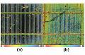
Magnetron-sputtered ZnO:Al is often used as a front contact in thin film silicon solar cells due to its transparent conductive oxide (TCO) properties that allow texturization by chemical etch processes to introduce light trapping. The transparency, conductivity, and surface texture after etching depend strongly on the sputtering conditions. Consequently, the typical preparation method is to find the right balance in TCO properties and light scattering, leading to a very narrow sputtering parameter window. It is preferable to separate the electro optical optimization from that of texturization to allow for a larger process window and improve ZnO:Al film properties further. This paper presents some methods of controlling the surface features using various mixtures of two step etching processes in aqueous solutions of HF and HCl. Results include methods for controlling the density of craters, texturizing compact ZnO:Al films, and fabricating novel modulated surfaces with more than one characteristic feature size. The two step etch process enables the creation of good surface textures even on high rate material that, via state of the art HCl etching, tend to lead to poor solar cell performance.
Premium
Cell Processing, Photovoltaics International Papers
A hydrogenated amorphous Si (a-Si:H) film, combined with a silicon nitride (SiNx:H) capping layer and a post-deposition anneal, can hugely enhance the surface passivation on crystalline silicon wafers. In this work, the influence of various deposition temperatures of a-Si:H films on the thermal stability of a-Si:H/SiNx:H stacks and a possible mechanism are discussed. Both minority carrier lifetime measurement and grazing-angle XRD were employed to study the thermal stability of a-Si:H/SiNx:H stacks, and the results are interpreted in terms of dihydrides concentration and epitaxial crystallization. With an appropriate thermal treatment, the a-Si:H film deposited at 130°C and capped by SiNx:H showed better passivation performance than 200°C-deposited a-Si:H/SiNx:H stacks, but under an excessive thermal budget the former showed more severe degradation of carrier lifetime. The more dihydride-rich composition within 130°C-deposited a-Si:H/SiNx:H stacks could be regarded as providing more effective intermediates for hydrogen interchanges, but on the other hand, it is also more susceptible to epitaxial crystallization.
Premium
Photovoltaics International Papers, Thin Film
Highly conductive transparent films are of significant interest in the field of thin-film photovoltaics. The solar cell type defines the necessary properties of the TCO used, as, besides the obvious qualities of transparency and conductivity, stability and morphology are important. The most significant properties of these aspects for front contacts in amorphous/microcrystalline silicon tandem, CIGS and CdTe solar cells are presented in this paper. Commonly used deposition techniques like CVD and sputter technology are described herein, focusing on particular techniques like SnO2:F and ZnO:B (CVD) and ZnO:Al (sputtering). New developments of deposition methods are also discussed.
Premium
Cell Processing, Photovoltaics International Papers
A selective emitter is a doping layer that is heavily doped beneath the electrode and lightly doped in between the electrode grids. One of the disadvantages of conventional selective-emitter techniques is the need for a high phosphorus surface concentration to obtain low contact resistance and limit the shunts in the emitter. Effective emitter passivation below the contact is difficult because of the use of emitters with low sheet resistances and high doping concentrations. In this study, the selective emitter in the optimized light/light sheet-resistance combination was formed to reduce recombination under the metal contact. The fabrication of optimized light/light doped emitters was performed using a single-step diffusion process. Besides the benefit of low surface recombination for light/light combination, this approach also removes the need for a very precise alignment between the opened emitter pattern and the front screen-printed silver fingers. This work illustrates the achievement of an efficiency improvement of more than 0.4% absolute in large-scale production for selective emitter solar cells.
Premium
Cell Processing, Photovoltaics International Papers
The workhorse of the photovoltaic industry, crystalline-silicon solar cells, continues to have additional headroom for conversion efficiency improvement as well as decreased production costs. As some companies have already demonstrated, clear pathways exist to bring about the achievement of >20%-efficient monocrystalline cells through the use of existing and novel production techniques. A newcomer to the solar cell and module sector, Suniva, has rapidly become a volume manufacturer using innovations originally developed at the University Center of Excellence in Photovoltaics (UCEP) at the Georgia Institute of Technology. This paper discusses the company’s first- and second-generation production technologies, including the implementation of ion implantation as a high-volume process, as well as details of cell-making approaches in the development stage.

Subscribe to Newsletter

Upcoming Events

Solar Media Events
May 21, 2025
London, UK
Solar Media Events
June 17, 2025
Napa, USA
Solar Media Events
July 1, 2025
London, UK
Solar Media Events
July 1, 2025
London, UK
Solar Media Events
July 8, 2025
Asia