Photovoltaics International Papers

Premium
Cell Processing, Photovoltaics International Papers
A recent spate of solar cell efficiency gains and record results underline the continued efforts to boost conversion efficiencies, which are at the core of reducing cost-per-watt goals. However, bringing such technology into the mainstream volume production world at little or no increase in manufacturing cost will prove more challenging. This paper takes a look at the current mainstream c-Si cell metallization efficiency developments that are starting to enter volume production with a promise of 20% cell efficiencies and low manufacturing costs.
Premium
Fab & Facilities, Photovoltaics International Papers
This paper presents and discusses the merits of layout, systems and options for exhaust treatments in PV cell production. Such treatments usually comprise central acid scrubbing, NOx scrubbing, Volatile Organic Compound (VOC) removal and several local treatments for dust, silane, and VOCs, while caustic scrubbing is an option for monocrystalline PV cell production. As direct and indirect major emissions from typical production steps have already been identified [1], this article focuses on a full emission pattern and identifies two sectors, VOC and NOx treatment, as most important for environmental impact analysis.
Premium
Photovoltaics International Papers, Thin Film
Thin-film solar photovoltaic technology offers the benefits of low-cost and high-volume production. Yet numerous thin-film PV startups have struggled in their efforts to commercialize complex, expensive production technologies, as production ramps have taken longer than expected, and venture capital and other sources of funding have run dry. This article describes a proprietary cadmium telluride (CdTe) thin-film module production process commercialized by Abound Solar: heated-pocket deposition (HPD) of the semiconductor layer, and the replacement of a traditional lamination process with a novel edge seal. The simple production process has resulted in a fast ramp of module efficiency and throughput. The paper will also describe how the process also results in fast throughput, high yields, and low manufacturing and capital equipment costs.
Premium
Market Watch, Photovoltaics International Papers
Mainland France’s photovoltaics market is substantially different from the situation in the country’s overseas Départements (DOM) and Corsica. Feed-in tariffs, tax breaks, financing and market players all differ in these territories. This paper takes a look at France’s mainland market, providing a projection for the country’s future market and some resources for more information on the DOM and Corsican markets [1].
Premium
Photovoltaics International Papers, PV Modules
Solar enterprises will each be faced with the occasional surplus or lack of solar modules in their lifetimes. In these instances, it is useful to adjust these stock levels at short notice, thus creating a spot market. Spot markets serve the short-term trade of different products, where the seller is able to permanently or temporarily offset surplus, while buyers are able to access attractive offers on surplus stocks and supplement existing supply arrangements as a last resort.
Premium
Photovoltaics International Papers, Power Generation
PV industry module and component manufacturers have brought down costs significantly over the last four years. This trend is clearly evident as most publicly traded companies continue to grow revenue despite falling module and component prices. However, it is far less clear how downstream system integrators are handling the drop in system prices and contributing to value creation. System prices are generally higher in the U.S. than in Europe, despite lower module prices in the U.S. This disparity often raises questions on the part of European PV professionals where these costs come from, and secondly, what have U.S. system integrators done to reduce costs. This two-part series will shed light on how U.S. system integrators have undertaken tremendous efforts to decrease cost and add value through innovation by focussing on labour-intensive value creation in the downstream segment. Part I will focus on the residential market segment by delving into activity cost savings through innovation in engineering and construction, while Part II will illustrate how changes in sales, rebates, interconnection, and the supply-chain management over the last five years have reduced costs.
Premium
Materials, Photovoltaics International Papers
“Handle with care” – this world-renowned warning sign is inherently printed on every wafer until it is safely wrapped into a finished module – and for good reason. Despite the declining price of silicon and the improved manufacturing methods, the raw wafer still has a major share in the overall cost of a module. If we assume an average wafer price of €2.70 for a 156mm multicrystalline wafer, the finished cell will cost about €4.00. Adding in the module manufacturing costs, a cell in a typical module will cost €5.00. Hence, the wafer accounts for more than 50% of the total manufacturing costs, and as such is key to optimizing the costs in the solar value chain for crystalline photovoltaic products. This paper offers some guidelines on the wet wafer separation process that are intended to aid in minimizing the cost associated with wafer breakage.
Premium
Fab & Facilities, Photovoltaics International Papers
Canada is aggressively pursuing solar photovoltaic manufacturing. Ontario, the province leading the charge, is already the manufacturing hub for other products in Canada and currently boasts one of the most generous feed-in tariffs in the world. This incentive is closely tied to domestic content restrictions in order to foster Canadian photovoltaic manufacturing. In addition, a host of other tax incentives and research and development stimulus packages are making Canada an increasingly popular destination for both established manufacturers and start-up companies.
Premium
Cell Processing, Photovoltaics International Papers
Advanced Process Control (APC) has become an indispensable cornerstone of today’s semiconductor manufacturing. With roots in chemical processing, APC has not only proven itself in semiconductor manufacturing, but has potential to enhance yield in adjacent industries, such as photovoltaics. This paper gives a short introduction to APC, including its key elements, and proceeds to illustrate examples and success stories from the application of APC in semiconductor manufacturing. Based on these application examples, the lessons learned are summarized and the potentials of APC for PV are derived.
Premium
Photovoltaics International Papers, PV Modules
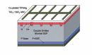
Encapsulant materials used in PV modules serve multiple purposes. They physically hold components in place, provide electrical insulation, optically couple superstrate materials (e.g., glass) to PV cells, protect components from mechanical stress by mechanically de-coupling components via strain relief, and protect materials from corrosion. To do this, encapsulants must adhere well to all surfaces, remain compliant, and transmit light after exposure to temperature, humidity, and UV radiation histories. Encapsulant materials by themselves do not completely prevent water vapour ingress [1-3], but if they are well adhered, they will prevent the accumulation of liquid water providing protection against corrosion as well as electrical shock. Here, a brief review of some of the polymeric materials under consideration for PV applications is provided, with an explanation of some of their advantages and disadvantages.

Subscribe to Newsletter

Upcoming Events

Media Partners, Solar Media Events
May 7, 2025
Munich, Germany
Solar Media Events
May 21, 2025
London, UK
Solar Media Events
June 17, 2025
Napa, USA
Solar Media Events
July 1, 2025
London, UK
Solar Media Events
July 1, 2025
London, UK