By Björn Rau, Technology Manager / Deputy Director, Helmholtz-Zentrum Berlin für Materialien und Energie GmbH/PVcomB; Felice Friedrich, Head of Analytics Group, Technical University Berlin/PVcomB; Niklas Papathanasiou, Head of CIGS Solar Cell Development, Helmholtz-Zentrum Berlin für Materialien und Energie GmbH/PVcomB; Christof Schultz, Engineer, HTW Laser Research Group, University of Applied Sciences Berlin (HTW)/PVcomB; Bernd Stannowski, Head of TF Si R&D Group, Helmholtz-Zentrum Berlin für Materialien und Energie GmbH/PVcomB; Bernd Szyszka, Professor, Technical University Berlin/PVcomB; Rutger Schlatmann, Helmholtz-Zentrum Berlin für Materialien und Energie GmbH/PVcomB, Director, University of Applied Sciences Berlin (HTW)/PVcomB
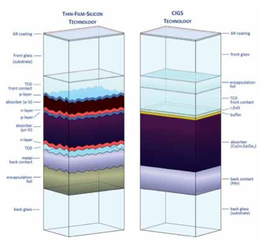
Thin-film PV modules are one of the most sustainable options for the generation of electricity, with low material consumption and short energy-payback times. Both of these factors are essential for paving the way towards a terawatt PV market. However, the cost-competitive production of PV modules has become extremely difficult, and module producers are facing huge challenges. A rapid technology transfer from research to industry is therefore required in order to introduce innovations for lower production costs and higher conversion efficiencies. At the Competence Centre Thin-Film- and Nanotechnology for Photovoltaics Berlin (PVcomB), founded by the Helmholtz-Zentrum Berlin (HZB) and the Technical University Berlin, two R&D lines for 30 x 30cm2 modules based on thin-film silicon and copper indium gallium (di)selenide (CIGS) respectively are operated. Robust baseline processes on a high efficiency level, combined with advanced process and device analytics, have been established as a basis for the introduction and development of further innovative technology steps, and their transfer to industry.