By Thomas Behm, TU Bergakademie Freiberg, Institute of Experimental Physics; Wolfgang Fütterer, TU Bergakademie Freiberg, Institute of Experimental Physics; Claudia Funke, TU Bergakademie Freiberg, Institute of Experimental Physics; Steffi Kaminski, Research Scientist, TU Bergakademie Freiberg, Institute of Experimental Physics; Hans-Joachim Möller, Professor, TU Bergakademie Freiberg, Institute of Experimental Physics; Romy Rietzschel, TU Bergakademie Freiberg, Institute of Experimental Physics; Thomas Wagner, TU Bergakademie Freiberg, Institute of Experimental Physics
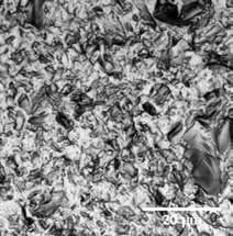
This paper discusses the wire sawing process and its impact on the wafer surface and subsurface. Surface damage is found to be the main determinant in wafer stability, while an outline of the sawing parameters that have a strong influence on the surface and subsurface damage is presented. The results indicate how it is possible to decrease the breakage rate of wafers and improve the homogeneity (e.g. TTV) of wafer surfaces. A further goal in the development of the wire sawing process is to successfully reduce material consumption. This can be achieved by sawing thinner wafers with thinner wires, which leads to a reduction of the kerf loss per produced silicon surface. The second option is to increase the material yield by decreasing the wafer breakage. It will be shown that silicon wafers with less and shorter cracks and smoother surfaces will give a higher yield, while proceeding to discuss some of the important factors that affect the microcrack formation.