By Tim Giesen, Project Manager, Institute for Manufacturing Engineering and Automation IPA; Raphael Adamietz, Project Manager, Institute for Manufacturing Engineering and Automation IPA; Guido Kreck, Institute for Manufacturing Engineering and Automation IPA; Tobias Iseringhausen, Project Manager, Institute for Manufacturing Engineering and Automation IPA; Roland Wertz, Manager, Institute for Manufacturing Engineering and Automation IPA
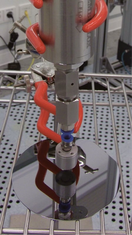
The positive expectations for the global PV market are driven by state-of-the-art PV products which have become economically attractive because of technical optimization. Nonetheless, scientists and engineers face the next generation of wafer-based PV technologies in terms of processing recipes and automation techniques. In this paper, motivations, challenges and advances relating to the handling of ultrathin PV substrates are identified for future application. A brief look out of the PV box at neighbouring disciplines in high-tech sectors will also be taken. The differences and advances in the automated handling of ultrathin substrates will be highlighted as well as the difficulties for transportation. The advanced production challenges of a gripperbased
substrate movement will be accompanied by increased cleanliness requirements, as test results from the Fraunhofer IPA automation lab show.