By Douglas M. Powell, Massachusetts Institute of Technology; David P. Fenning, Massachusetts Institute of Technology; Jasmin Hofstetter, Massachusetts Institute of Technology; Jean-François Lelièvre, Instituto de Energía Solar, Universidad Politécnica de Madrid; Carlos del Cañizo, Instituto de Energía Solar, Universidad Politécnica de Madrid; Tonio Buonassisi, Heads the Photovoltaic Research Laboratory, Massachusetts Institute of Technology
Coupled device and process simulation tools, collectively known as technology computer-aided design (TCAD), have been used in the integrated circuit industry for over 30 years. These tools allow researchers to quickly home in on optimized device designs and manufacturing processes with minimal experimental expenditures.
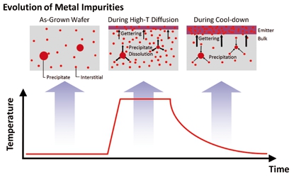
The PV industry has been slower to adopt these tools, but is quickly developing competency in using them. This paper introduces a predictive defect engineering paradigm and simulation tool, while demonstrating its effectiveness at increasing the performance and throughput of current industrial processes. The impurity-to-efficiency (I2E) simulator is a coupled process and device simulation tool that links wafer material purity, processing parameters and cell design to device performance. The tool has been validated with experimental data and used successfully with partners in industry. The simulator has also been deployed in a free web-accessible applet, which is available for use by the industrial and academic communities.