By Mark Schumann, Fraunhofer ISE; Teresa Orellana Pérez, Fraunhofer ISE; Stephan Riepe, SIMTEC Laboratory, Fraunhofer ISE
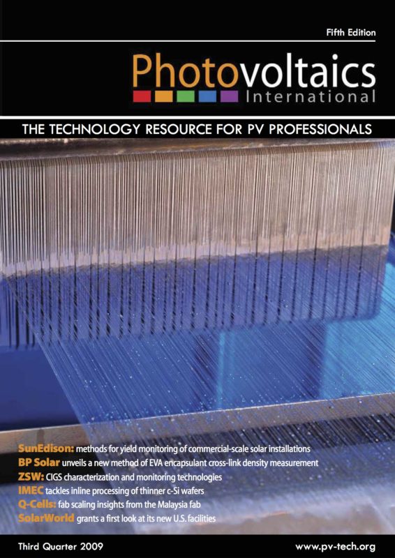
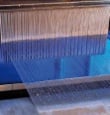
The process of wafering silicon bricks into wafers represents about 20% of the entire production cost of crystalline silicon solar cells. In this paper, the basic principles and challenges of the wafering process are discussed. The multi-wire sawing technique used to manufacture wafers for crystalline silicon solar cells, with the reduction of kerf loss currently representing about 50% of the silicon, presents a major challenge for further research efforts. Another relevant field of research is the reduction of wafer thickness in order to obtain more wafers per millimetre of brick length. The last subject that is addressed in this paper is the general optimization of the wafer surface and geometry, as the multi-wire saw cutting process influences the mechanical properties of the wafers and can have further effects on subsequent process steps.