Materials

Premium
Materials, Photovoltaics International Papers
Reduction of silicon wafer thickness without increasing the wafer’s strength can lead to a high fracture rate during subsequent handling and processing steps. The cracking of solar cells has become one of the major sources of solar module failure and rejection. Hence, it is important to evaluate the mechanical strength of silicon solar wafers and influencing factors. The purpose of this work is to understand the fracture behaviour of multicrystalline silicon wafers and to obtain information regarding the fracture of solar wafers and solar cells. The effects on silicon wafer strength of saw damage and of grain size, boundaries and triple junctions are investigated, while the effects of surface roughness and the damage layer removal process are also considered. Significant changes in fracture strength are found as a result of different silicon wafer crystallinity and surface roughness. Results indicate that fracture strength of a processed silicon wafer is mainly affected by the following factors: the saw-damage layer thickness, surface roughness, cracks/ defects at the edges and the number of grain boundaries – which all serve as possible crack initiation points. The effects of metallization paste type and firing conditions on the strength of solar cells are also considered, with findings indicating that the aluminium paste type and firing conditions influence the strength of solar cells.
Premium
Materials, Photovoltaics International Papers
With more than 80% of PV module demand being satisfied by crystalline-based modules, the health of the silicon and wafer supply chain is of vital importance to the overall PV industry. This paper reviews the overall materials value chain from the manufacture of PV silicon to the wafer, prepared for manufacture of the cell. A glimpse is provided of the various market dynamics that exist in the supply chain, as well as the technology trends that influence or threaten the supply of wafers. Although the manufacturing routes are mature and well established, we also take a look at the possibility of novel and disruptive technologies altering the overall supply landscape.
Premium
Materials, Photovoltaics International Papers
This paper discusses the wire sawing process and its impact on the wafer surface and subsurface. Surface damage is found to be the main determinant in wafer stability, while an outline of the sawing parameters that have a strong influence on the surface and subsurface damage is presented. The results indicate how it is possible to decrease the breakage rate of wafers and improve the homogeneity (e.g. TTV) of wafer surfaces. A further goal in the development of the wire sawing process is to successfully reduce material consumption. This can be achieved by sawing thinner wafers with thinner wires, which leads to a reduction of the kerf loss per produced silicon surface. The second option is to increase the material yield by decreasing the wafer breakage. It will be shown that silicon wafers with less and shorter cracks and smoother surfaces will give a higher yield, while proceeding to discuss some of the important factors that affect the microcrack formation.
Premium
Materials, Photovoltaics International Papers
The minority carrier lifetime is a key parameter for the performance of solar cells as it characterizes the electrical quality of the semiconductor material. Consequently, accurate and reliable methods to determine the minority carrier lifetime are of enormous interest for both practical process control and the evaluation of the potential and limitations of a specific cell concept. Due to its importance, many different lifetime measurement techniques have been developed and used over the past few decades. This paper aims to present and discuss the most common measurement methods on the one hand, while attempting to shed light on some recent developments on the other. The determination of the minority carrier lifetime of crystalline silicon thin-film (cSiTF) material is illustrated as an example of interest for those who are already familiar with standard lifetime characterization.
Premium
Materials, Photovoltaics International Papers
The next generation of industrial silicon solar cells aims at efficiencies of 20% and above. To achieve this goal using ever-thinner silicon wafers, a highly effective surface passivation of the cell, front and rear, is required. In the past, finding a suitable dielectric layer providing a high-quality rear passivation has been a major challenge. Aluminium oxide (Al2O3) grown by atomic layer deposition (ALD) has only recently turned out to be a nearly perfect candidate for such a dielectric. However, conventional ALD is limited to deposition rates well below 2nm/min, which is incompatible with industrial solar cell production. This paper assesses the passivation quality provided by three different industrially relevant techniques for the deposition of Al2O3 layers, namely high-rate spatial ALD, plasma-enhanced chemical vapour deposition (PECVD) and reactive sputtering.
Premium
Materials, Photovoltaics International Papers
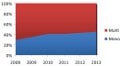
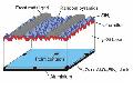
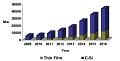
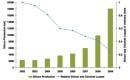
Despite the financial crisis and present credit crunch, photovoltaic materials markets experienced only a temporary slide in demand in 2009, with the overall outlook remaining optimistic. This paper presents a strategic analysis review for the materials used in photovoltaic modules, essentially materials for encapsulant, frontsheet, backsheet and anti-reflection coatings. Rising concerns about the need to reduce CO2 emissions and increase the use of renewable energy sources worldwide will stimulate the global photovoltaic market. Feed-in tariffs and politically backed targets boosting renewable energy use will provide further impetus to the photovoltaic market. This, in turn, will have a positive ripple effect on the demand for photovoltaic materials; however, depending on the market share for technology used, i.e. crystalline or thin film for PV energy, the market for materials will be influenced, in addition to advantages and disadvantages of these materials that will influence their market share. With rising awareness about green trends, the future will lie in technologies that offer enhanced energy-efficient solutions at a low cost. Manufacturers who offer products with optimum performance while remaining price-orientated will be poised to gain substantial market share.
Premium
Materials, Photovoltaics International Papers
“Handle with care” – this world-renowned warning sign is inherently printed on every wafer until it is safely wrapped into a finished module – and for good reason. Despite the declining price of silicon and the improved manufacturing methods, the raw wafer still has a major share in the overall cost of a module. If we assume an average wafer price of €2.70 for a 156mm multicrystalline wafer, the finished cell will cost about €4.00. Adding in the module manufacturing costs, a cell in a typical module will cost €5.00. Hence, the wafer accounts for more than 50% of the total manufacturing costs, and as such is key to optimizing the costs in the solar value chain for crystalline photovoltaic products. This paper offers some guidelines on the wet wafer separation process that are intended to aid in minimizing the cost associated with wafer breakage.
Premium
Materials, Photovoltaics International Papers
This paper gives an overview of the French PHOTOSIL project that deals with the purification of metallurgical-grade (MG) silicon via different stages of upgraded metallurgical-grade (UMG) silicon to finally arrive at a purity level that is compatible with the requirements of the silicon-based PV industry. However, purified UMG silicon in general and by definition does not reach the ultra-high purity levels of electronic-grade (EG) silicon. Based on the PHOTOSIL project, this paper presents the typical technical challenges and problems encountered with less pure purified UMG silicon and how they were resolved, both during silicon purification and crystallization and the processing of solar cells.
Premium
Materials, Photovoltaics International Papers
The photovoltaic market, which is dominated by polysilicon-based crystalline solar cells, has been developing rapidly, with growth rates in the double-digit range for several years. In order to meet increasing demand for hyperpure polysilicon, manufacturers need to adhere to environmentally-friendly production processes with low energy consumption. This article highlights the key processes needed to manufacture hyperpure polycrystalline silicon and explores the related challenges and solutions for sustainable polysilicon production. Our findings prove that only an intelligent interaction of all necessary process steps fulfils the requirements for minimized production residue volumes and low energy consumption. Totally integrated production loops for all essential media are prerequisite to reach these targets. Once implemented, these highly efficient production processes serve as an excellent platform technology for the continued healthy growth of the PV industry.
Premium
Materials, Photovoltaics International Papers
Multicrystalline wafers are the workhorse of the PV industry, with approximately 60% of crystalline silicon solar cells made from the substrate. They offer cost advantages in the form of good conversion efficiencies, which should continue to improve as cell technology advances continue. However, wafer prices were acutely impacted by the fall in PV market demand in late 2008, which continued through most of 2009. With relatively high capital costs, continued pricing pressures and calls for greater quality and control, wafer producers are now set on a course that requires rigorous and sustainable production cost-reduction strategies to meet customer requirements. This paper focuses on strategies that can be adopted to address this need for tighter quality specifications that reduce manufacturing costs downstream and boost cell conversion efficiencies.

Subscribe to Newsletter

Upcoming Events

Solar Media Events
May 1, 2024
Dallas, Texas
Solar Media Events
May 21, 2024
Sydney, Australia