Photovoltaics International Papers

Premium
Materials, Photovoltaics International Papers
The PV industry is undergoing dramatic changes. Like a carnival ride gone dreadfully wrong, exhilaration has been supplanted by dread; joy has been replaced by fear. Just look around you – provided you are able to turn your head to defy the g-forces acting upon you as we bank and turn wildly along. You will see PV companies closing their doors for good. You will see extraordinarily talented people throughout the supply chain, shifting positions everywhere and looking for safe-haven jobs. And you will also see once-leading PV companies burning cash and losing their status as ‘bankable’. Everywhere we turn, we see companies in the supply chain shuttering production as if to balance markets.
Premium
Fab & Facilities, Photovoltaics International Papers
Several PV module producers have performed a carbon footprint analysis and published a sustainability report as part of their corporate social responsibility policy. Comparison of carbon footprint results is difficult because several international standards and life cycle assessment (LCA) databases are used. No product footprint category rules (PFCR) or product category rules (PCRs) for photovoltaics exist, so LCAs are performed with varying underlying assumptions. Furthermore, a fair comparison can only be made when all environmental footprints of a product are taken into account.
Premium
Cell Processing, Photovoltaics International Papers
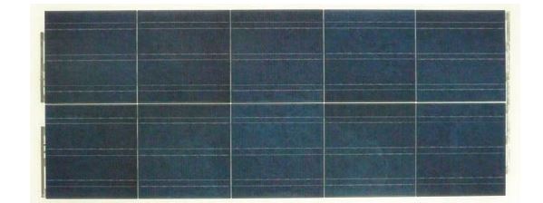
In the photovoltaics industry, contacts to crystalline silicon are typically formed by the firing of screen-printed metal pastes. However, the stability of dielectric surface passivation layers during the high-temperature contact formation has turned out to be a major challenge for some of the best passivating layers, such as intrinsic amorphous silicon. Capping of well-passivating dielectric layers by hydrogen-rich silicon nitride (SiNx), however, has been demonstrated to improve the thermal stability, an effect which can be attributed to the atomic hydrogen (H) diffusing out of the interface during firing, and passivating dangling bonds. This paper presents the results of investigations into the influence of two different dielectric passivation stacks on the firing stability, namely SiNy/SiNx (y < x) and Al2O3/SiNx stacks. Excellent firing stability was demonstrated for both stack systems. Effective surface recombination velocities of < 10cm/s were measured after a conventional co firing process on 1.5Ωcm p-type float-zone silicon wafers for both passivation schemes. On the solar cell level, however, better results were obtained using the Al2O3/SiNx stack, where an efficiency of 19.5% was achieved for a large-area screen-printed solar cell fabricated on conventional Czochralski-grown silicon.
Premium
Photovoltaics International Papers
The Unite d States and China are embroiled in what the New York Times has dubbed “the most politically charged trade case in many years”. Seven US-based crystalline silicon solar cell manufacturers have formed. The Coalition for American Solar Manufacturing (CASM), led by SolarWorld and First Solar (the identities of the five remaining members are yet to be disclosed). The CASM has accused Chinese manufacturers of violating global trade laws with its “anti-competitive trade aggression”.
Premium
Photovoltaics International Papers, PV Modules
This paper presents a new differential scanning calorimetry (DSC) method that allows the determination of the degree, or level, of crosslinking of ethylene-vinyl acetate (EVA) copolymers, including EVA films used as encapsulants for photovoltaic (PV) applications. This method can also determine additional characteristics of EVA, such as its weight per cent (wt %) vinyl acetate (VA) content and its fluidity. The paper describes the procedure and its application to EVA film samples laminated at 145°C, for different lengths of time in an industrial-type laminator for PV modules, as well as to EVA uncrosslinked samples of different composition and fluidity. The scope of the method compared to other characterization methods for the degree of crosslinking of EVA is discussed. An experimental comparison is also made to rheological and gel content methods.
Premium
Photovoltaics International Papers, PV Modules
This paper describes the technical concepts and current status of back-contact module technology. A back-contact module has the advantage of a higher conversion efficiency because of less shading of the front of the cell, fewer inactive areas in the module and lower series resistance in the interconnection. Aesthetically, back-contact modules are more attractive than standard modules. Furthermore, module manufacturing is gentler due to there being less cell handling during the process. The two main technical concepts related to back-contact modules – interconnector technology and printed circuit backsheet technology – are discussed in this paper. An overview is given of the production status of current back-contact module manufacturers to also show the significant potential of this technology in economic terms.
Premium
Photovoltaics International Papers, PV Modules
Photovoltaic (PV) modules and components are products which have to withstand the diverse effects of extreme conditions during their lifetime. The wide range of climatic conditions and possible mechanical stresses must be taken into account when designing a PV component. To assess whether the quality of a product is sufficient to withstand such influences, some international standards have been developed. TÜV Rheinland operates several ISO 17025-accredited laboratories worldwide for type approval testing of PV components – such as junction boxes, connectors and cables – as well as concentrating PV modules, flat-plate modules and solar thermal systems. Experience of testing PV components has been gained over the last 12 years, and even over the last 20 years in the case of PV modules. New developments in photovoltaics mean that continuous development and review of standards is necessary.
Premium
Photovoltaics International Papers, Thin Film
Sales of critical subsystems used in thin-film PV manufacturing equipment are expected to reach $324M in 2011, and the outlook is for this figure to grow by 3.74% in 2012 to $336M. This expectation is going against the trend for the industry as a whole, which is predicted to decline next year as revenues from cell and module manufacturing weaken. The reason for this countermovement is the opportunities available to manufacturers who are willing to invest in the latest thin-film PV equipment to drive down costs and force unprofitable competitors out of business. While the same opportunities exist for crystalline silicon manufacturing, the number of well-resourced companies signalling their intention to invest in thin-film technologies should ensure a positive year for suppliers of equipment and critical subsystems to this segment of the industry.
Premium
Photovoltaics International Papers, Thin Film
In terms of material properties, plasma-enhanced chemical vapour deposition (PECVD) of ZnO has advantages over sputtering techniques, due to the variety of available precursors, and the different dopants for achieving certain levels of n-type and, controversially discussed, p-type transparent conductive oxides (TCOs) on various substrate materials. This paper considers the deposition of boron-doped zinc oxide for n-type TCO-application on substrates of dimensions up to 50×50cm2 and at a temperature range of 50 to 450°C using a PECVD reactor with a plasma frequency of 13.56MHz. The materials’ characteristics such as transparency, carrier concentration and structural properties are discussed as a function of the deposition parameters. The deposition temperature strongly affects the crystallographic and morphological appearance of the deposited thin films, which was investigated using field emission scanning electron microscope (FESEM) and X-ray diffraction (XRD) methods. The electronic band structure-dependent characteristics were studied using ultraviolet-visible (UV-vis) spectroscopy and Hall measurements. Secondary ion mass spectrometry (SIMS) measurements complete the characterization methods for qualitatively verifying the incorporation of dopants and impurities. Results are reported for columnar-grown boron-doped ZnO with optical transparency greater than 80% in the visible range and a maximum carrier concentration of 1020cm-3.
Premium
Photovoltaics International Papers, Thin Film
Because of its attractive electronic and optical properties, zinc oxide (ZnO) has found widespread use as a front and back electrode in commercial solar cells. ZnO can be deposited on glass using a variety of different methods, of which vacuum-based techniques are the most commonly used in industrial applications. Aluminium-doped sputtered ZnO:Al (AZO) has been studied intensively for use as a front contact in a-Si/μc-Si tandem cells. The implementation of AZO in series production has been hindered by reproducibility issues stemming from the combination of deposition and subsequent etching steps that are necessary to tune the ‘haze’ of the layers for optimal light scattering. Boron-doped ZnO:B (BZO), deposited by low-pressure chemical vapour deposition (LPCVD), has become a cost-effective option for module manufacturers, since the desired layer morphology can be produced as grown without the need of post-growth chemical etching. This paper addresses the different aspects of using AZO and BZO layers as front contacts for a-Si/μc-Si tandem modules fabricated in series production. The properties of the underlying ZnO layers put restrictions on the layer properties and process parameters that are used in the deposition of a-Si and μc-Si.

Upcoming Events

Solar Media Events
February 3, 2026
London, UK
Upcoming Webinars
February 18, 2026
9am PST / 5pm GMT
Solar Media Events
March 24, 2026
Dallas, Texas
Solar Media Events
April 15, 2026
Milan, Italy
Solar Media Events
June 16, 2026
Napa, USA