By Bram Hoex, Director and Group Leader in the Silicon PV Cluster, SERIS, National University of Singapore; Debajyoti Sarangi, Senior Research Scientist, SERIS, National University of Singapore; Edwin Carmona, Process Engineer in the PV Production Group, SERIS, National University of Singapore; Jason Avancena, Process Engineer in the PV Production Group, SERIS, National University of Singapore; Jessen Cunnusamy, Engineer on Crystalline Silicon Solar Cells, SERIS, National University of Singapore; Kishan Devappa Shetty, Research Engineer on Crystalline Silicon Solar Cells, SERIS, National University of Singapore; Matthew Boreland, Director of the Silicon PV Cluster, SERIS, National University of Singapore; Prabir Kanti Basu, Senior Research Scientist in the Silicon PV Cluster, SERIS, National University of Singapore; Sandipan Chakradorty, Research Fellow in the Silicon PV Cluster, SERIS, National University of Singapore; Ziv Hameiri, Research Fellow in the Silicon PV Cluster, SERIS, National University of Singapore
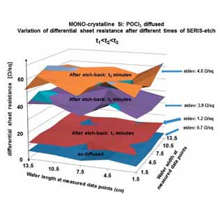
Emitter formation is one of the most critical processes in the fabrication of silicon wafer solar cells. The process for standard emitter formation adopted in the photovoltaic industry is tube-based diffusion, using phosphorus oxychloride as the dopant source. A potentially low-cost alternative that typically results in lower solar cell efficiencies is in-line diffusion, using phosphoric acid as the dopant source. The Solar Energy Research Institute of Singapore (SERIS) recently developed a technique called the ‘SERIS etch’, a non-acidic etch-back process technology that provides a controllable, uniform and substantially conformal etch-back suitable for solar cell processing. By using the SERIS etch, efficiencies of up to 18.7% have been demonstrated for omogeneous-emitter silicon wafer cells; a 0.4%abs efficiency improvement has also been achieved for a unique selective-emitter approach exploiting this novel etch. All work was carried out on industrial-grade p-type Cz wafers with conventional screen-printed metallization and a full-area aluminium back-surface field (Al-BSF). With Al local BSF (LBSF) homogeneous-emitter solar cells, efficiencies of 19.0% were achieved using in-line emitter diffusion and the SERIS etch, a 0.7%abs efficiency increase over the baseline efficiency at the time. To the authors’ knowledge, these are the highest solar cell efficiencies ever reported for in-line-diffused silicon solar cells. Moreover, the SERIS etch is a costeffective alternative to generating pyramid-textured surfaces without using conventional metal-assisted siliconetching processes.