Technical Papers

Premium
Photovoltaics International Papers, Thin Film
This paper presents fluorescence detection as a new tool for the investigation of the degradation of EVA. The superior sensitivity of the setup contained herein allows an early assessment of the changes of the EVA after only 20 hours of damp-heat exposure. A newly developed scanning system allows the spatially resolved inspection of entire PV modules. Degradation of the encapsulants was detected after two years’ outdoor exposure, as was the effect of cracks in c-Si cells, which coincide well with cracks made visible by electroluminescence.
Premium
Photovoltaics International Papers, Power Generation
Despite the collapsed Spanish market and the general state of the world’s economy, the past year was not a bad year at all from the perspective of installed power capacity of large-scale PV power plants. Installed power capacity surpassed expectations while also bringing new markets into the spotlight, which means that the traditional market leaders of Spain, Germany and the U.S. are no longer the only ‘key’ markets. With the exception of Germany, the past year’s most noteworthy market boost was seen in the Czech Republic and Italy, with similar shake-ups seen in the Asian tiger countries of China and India. With many large-scale PV power plants recently brought into commission in these countries, China and India are brimming with potential for the near future.
Premium
Materials, Photovoltaics International Papers
This paper gives an overview of the French PHOTOSIL project that deals with the purification of metallurgical-grade (MG) silicon via different stages of upgraded metallurgical-grade (UMG) silicon to finally arrive at a purity level that is compatible with the requirements of the silicon-based PV industry. However, purified UMG silicon in general and by definition does not reach the ultra-high purity levels of electronic-grade (EG) silicon. Based on the PHOTOSIL project, this paper presents the typical technical challenges and problems encountered with less pure purified UMG silicon and how they were resolved, both during silicon purification and crystallization and the processing of solar cells.
Premium
Cell Processing, Photovoltaics International Papers
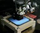
Solar cells are generally built in a process facility, often a turnkey line, where high throughput, minimum handling, and lowest cost are dominant factors. There are many complementary metal oxide semiconductor (CMOS) lines in the semiconductor industry – probably more than the number of turnkey lines – where yield, reliability, and device size and complexity are major issues, where millions of chips are made with very close tolerance, and the cost of importance is that of the finished chip. The possibility of using or converting a CMOS line for building Si solar cells has been considered by many in the past [2]. These lines have advantages such as sophisticated and highly developed automated equipment, frequent in-process metrology and quality control, and a high degree of flexibility as well as highly advanced shop floor control systems. The major disadvantages are cost and low throughput. This paper will discuss the differences, advantages, and disadvantages of CMOS and turnkey lines and show preliminary results for Si cells made in the CMOS line.
Premium
Photovoltaics International Papers, PV Modules
Cell interconnection is recognized as the most critical process with respect to module production yield. If the process is not carefully controlled, cell cracking and subsequent breakage may occur. Many manufacturers promise breakage rates below 0.3-0.5% on their tabber-stringers, which applies for cells above 160-180µm thickness that are free from initial cracks. In real production, this figure strongly depends on materials, process parameters and throughput. This paper outlines some approaches that should be taken to avoid high levels of breakage in the cell interconnection process.
Premium
Photovoltaics International Papers, Thin Film
With the never-ending need to reduce production costs, interest in atmospheric deposition techniques is steadily increasing. Even though atmospheric deposition is not new to photovoltaics, and in some cases is actually required to get the best cell performance, many of the fabrication processes for photovoltaic cells are vacuum-based. Due to the diversity in atmospheric deposition techniques available, there are opportunities for applications in thin film and patterned deposition. This paper discusses some of the deposition techniques and their applications, benefits and drawbacks.
Premium
Market Watch, Photovoltaics International Papers
The upper and lower houses of the German parliament took their time finding a compromise on the degression of PV tariffs. Cutbacks were finally decided on at the start of July. The German PV market is now headed for another record-breaking year in 2010 despite or maybe even as a result of these reductions. EuPD Research, the market research institute, is making a conservative projection of approximately 5.5GW in newly-installed capacity. Nevertheless, pressure is set to increase, particularly on German solar companies. New marketing strategies have to be developed in the mid-term in order to survive and explore new segments in the long term.
Premium
Materials, Photovoltaics International Papers
The photovoltaic market, which is dominated by polysilicon-based crystalline solar cells, has been developing rapidly, with growth rates in the double-digit range for several years. In order to meet increasing demand for hyperpure polysilicon, manufacturers need to adhere to environmentally-friendly production processes with low energy consumption. This article highlights the key processes needed to manufacture hyperpure polycrystalline silicon and explores the related challenges and solutions for sustainable polysilicon production. Our findings prove that only an intelligent interaction of all necessary process steps fulfils the requirements for minimized production residue volumes and low energy consumption. Totally integrated production loops for all essential media are prerequisite to reach these targets. Once implemented, these highly efficient production processes serve as an excellent platform technology for the continued healthy growth of the PV industry.
Premium
Cell Processing, Photovoltaics International Papers
A recent spate of solar cell efficiency gains and record results underline the continued efforts to boost conversion efficiencies, which are at the core of reducing cost-per-watt goals. However, bringing such technology into the mainstream volume production world at little or no increase in manufacturing cost will prove more challenging. This paper takes a look at the current mainstream c-Si cell metallization efficiency developments that are starting to enter volume production with a promise of 20% cell efficiencies and low manufacturing costs.
Premium
Photovoltaics International Papers, Thin Film
Thin-film solar photovoltaic technology offers the benefits of low-cost and high-volume production. Yet numerous thin-film PV startups have struggled in their efforts to commercialize complex, expensive production technologies, as production ramps have taken longer than expected, and venture capital and other sources of funding have run dry. This article describes a proprietary cadmium telluride (CdTe) thin-film module production process commercialized by Abound Solar: heated-pocket deposition (HPD) of the semiconductor layer, and the replacement of a traditional lamination process with a novel edge seal. The simple production process has resulted in a fast ramp of module efficiency and throughput. The paper will also describe how the process also results in fast throughput, high yields, and low manufacturing and capital equipment costs.

Subscribe to Newsletter

Upcoming Events

Solar Media Events
May 21, 2025
London, UK
Solar Media Events
June 17, 2025
Napa, USA
Solar Media Events
July 1, 2025
London, UK
Solar Media Events
July 1, 2025
London, UK
Solar Media Events
July 8, 2025
Asia