By Jonas Bartsch, Head of the Plating Process Technology Team, Fraunhofer ISE; Andreas Brand, Production Technology and Quality Assurance Department, Fraunhofer ISE; Dirk Eberlein, Project Engineer, Photovoltaic Modules Group, Fraunhofer ISE; Andrew Mondon, Fraunhofer ISE; Carola Völker, TestLab PV Modules facility, Fraunhofer ISE; Marco Tranitz, Fraunhofer ISE; Martin Graf, Fraunhofer ISE; Jan Nekarda, Laser Process Technology Group Leader, Fraunhofer ISE; Ulrich Eitner, Photovoltaic Modules Group, Fraunhofer ISE; Daniel Philipp, Head of the Module Testing Group, Fraunhofer ISE; Markus Glatthaar, Head of the Novel Processes Department, Fraunhofer ISE
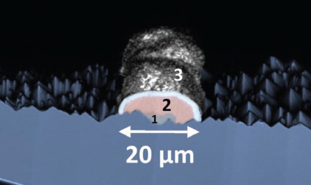
This paper presents the first 60-cell module results from a very simple process scheme for creating fully plated nickel-copper contacts on crystalline silicon solar cells. Standard Cz back-surface field (BSF) cells are processed in a completely analogous way to the standard process sequence up to and including rear-side screen printing. After a firing step for BSF formation, the front-grid positions are defined by picosecond pulse laser ablation and plated with nickel, copper and silver; this is followed by a short thermal anneal. Cell classification produces a very neat efficiency distribution of 19.6±0.1%. Solder and peel testing shows this approach to be competitive with standard screen-printed contacts in terms of adhesion. A batch of 60-cell modules were fabricated from the cells in a standard automated tabber-stringer system and subjected to thermal cycling and damp heat testing as part of the IEC 61215 reliability test sequence. The modules passed the test sequence without showing any signs of electrical degradation caused by, for example, copper diffusion.


