By María Recamán Payo, imec, Leuven, Belgium; Izabela Kuzma-Filipek, imec, Leuven, Belgium; Filip Duerinckx, imec, Leuven, Belgium; Yuandong Li, imec, Leuven, Belgium; Emanuele Cornagliotti, imec, Leuven, Belgium; Angel Uruena, imec, Leuven, Belgium; Loic Tous, imec, Leuven, Belgium; Richard Russell, imec, Leuven, Belgium; Ali Hajjiah, Kuwait University, College of Engineering and Petroleum, Electrical Engineering Dept., Safat, Kuwait; Maarten Debucquoy, imec, Leuven, Belgium; Jozef Szlufcik, imec, Leuven, Belgium; Jozef Poortmans, imec, Leuven, Belgium; KU Leuven, Leuven, and University of Hasselt, Diepenbeek, Belgium
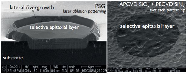
This paper gives an overview of the application of silicon epitaxy as a doping technology in bulk crystalline silicon solar cells. The large degree of flexibility in designing a doped profile in one process step, and the elegant way of locally creating doped regions, or simply achieving single-side doping by selective epitaxy, are presented. Other advantages – such as the absence of subsequent steps to drive in the doped region, to activate the dopants and to heal any damage or remove glassy layers – position the technology as a strong alternative to classical diffusion. Silicon epitaxy is possible on the flat and textured surfaces of solar material, and is compatible with cleaning sequences suited to industrial implementation. The integration of epitaxial layers in solar cells is capable of providing not only high efficiencies but also simplifications of the cell fabrication process, and, therefore, reductions in the cell cost of ownership (CoO). The proof of concept at the cell level has been demonstrated by the integration of boron-doped epitaxial emitters in n-type IBC and PERT solar cells: 22.8% efficiency for IBC (4cm2) and 21.9% for PERT (238.9cm2) devices have been obtained.