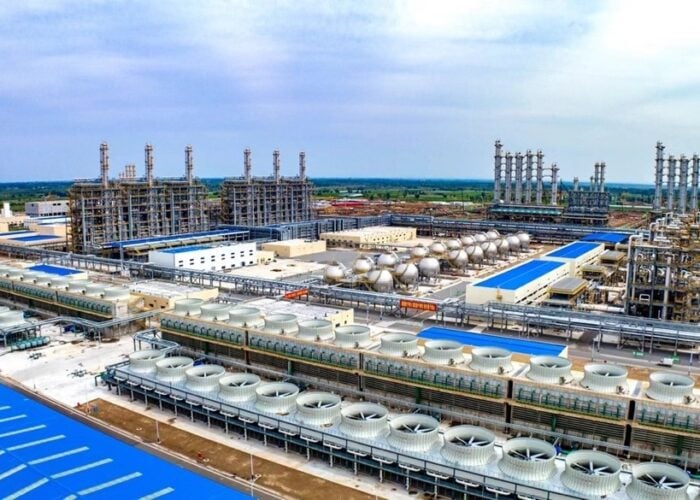
Dow Chemical announced that it had officially opened its Dow Seoul Technology Centre in Hwaseong, Gyeonggi-do. The R&D centre will focus on technological advances in display technologies and semiconductor-related applications including lithography, organic light-emitting diodes (OLED), display materials and advanced chip packaging.
The R&D centre will serve as the company’s global hub for its OLED research. The company noted that the facility sports a Nikon 193nm immersion scanner and 300mm tool cluster, which it states makes it the only photoresist supplier in the world with a 193i application and development facility in Korea.
Try Premium for just $1
- Full premium access for the first month at only $1
- Converts to an annual rate after 30 days unless cancelled
- Cancel anytime during the trial period
Premium Benefits
- Expert industry analysis and interviews
- Digital access to PV Tech Power journal
- Exclusive event discounts
Or get the full Premium subscription right away
Or continue reading this article for free
“This investment makes sense. Dow provides best-in-class technologies to enable faster, smaller and more powerful electronics and Korea is a global leader in the electronics market. With our new R&D center, we can deliver even more solutions for the fast-growing electronics industry – better serving our customers in Korea, but worldwide as well,” said Jerome Peribere, executive vice president of The Dow Chemical Company and president and chief executive officer of the Dow Advanced Materials Division.
Dow noted that with the completion of the R&D centre, it has invested over US$400 million in Korea over the last ten years for the establishment of manufacturing sites for semiconductor, display and LED technologies.

