A trio of companies is attempting to reduce the waste caused by wafer-sawing processes by growing crystalline silicon on relatively cheap foil. NREL has teamed up with DOE's Oak Ridge National Laboratory (ORNL) and c-Si thin-film technology company Ampulse with the aim of lowering the cost of solar panels.
The teams will use a chemical vapour deposition (CVD) process to grow high-quality silicon in thin layers on a metal foil developed by ORNL. Ampulse will design a full-scale production line that will support the long rolls of metal foil necessary to ensure the technology’s cost-effectiveness and will install the line in NREL's Process Development Integration Laboratory (PDIL).
Try Premium for just $1
- Full premium access for the first month at only $1
- Converts to an annual rate after 30 days unless cancelled
- Cancel anytime during the trial period
Premium Benefits
- Expert industry analysis and interviews
- Digital access to PV Tech Power journal
- Exclusive event discounts
Or get the full Premium subscription right away
Or continue reading this article for free
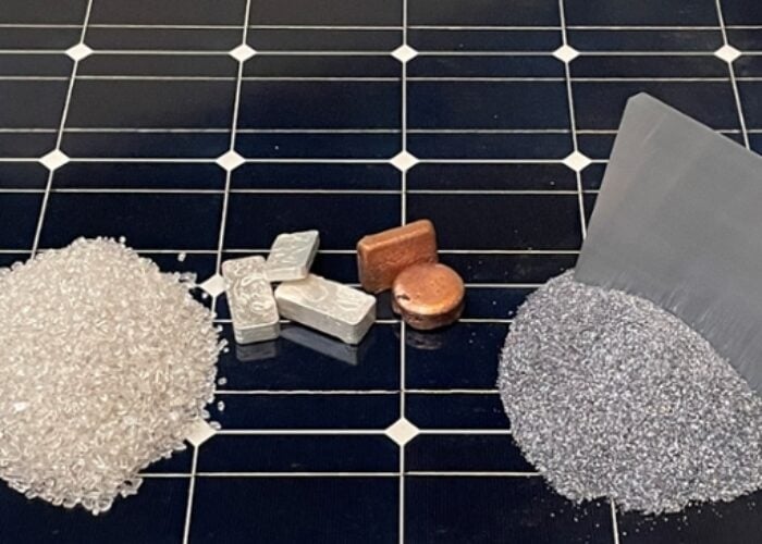
Today’s c-Si technology manufacturing process involved huge levels of wastage, as around half of the refined silicon is lost as dust in the wafer-sawing process. Furthermore, the wafer-sawing process can render incompatible as many as 6,000 wafers from a 2m boule of silicon. Wafers cut in this way are usually close to 10 times thicker than they need to be in order to convert the maximum amount of sunlight to electricity.
The Ampulse process does not require the creation of a feedstock, but works directly with the silane to grow the desired amount of silicon directly onto the foil substrate.
“[The process] goes straight from pure silicon-containing gas to high-quality crystal silicon film,” says Brent Nelson, operational manager for the PDIL at NREL. “The advantage is you can make the wafer just as thin as you need it — 10 microns or less.”
Further information on the collaborative effort is available here.