Ahead of the forthcoming PV CellTech 2020 Online conference on 27-29 October 2020, our head of research and Chair of the CellTech events, Dr. Finlay Colville, undertook an interview with one of the keynote speakers planned for the event, Dr. Sebastian Gatz, the Vice President of Crystalline Photovoltaics at leading equipment manufacturer Von Ardenne.
The questions were put forward in the interview by Finlay Colville.
Try Premium for just $1
- Full premium access for the first month at only $1
- Converts to an annual rate after 30 days unless cancelled
- Cancel anytime during the trial period
Premium Benefits
- Expert industry analysis and interviews
- Digital access to PV Tech Power journal
- Exclusive event discounts
Or get the full Premium subscription right away
Or continue reading this article for free
Von Ardenne has been developing high-throughput deposition tooling for the PV industry for many years now. What are the key drivers today, in 2020, for c-Si manufacturing, that differ from a few years ago?
Dr. Sebastian Gatz: “Efficiency was always a driver and resulted in the success story of PERC approaching 23%. Now we are facing the next step in GW scale manufacturing expansions. Two main routes can be identified here: TOPCon, following the PERC path, or HJT with 5% higher relative efficiencies. The investments made by cell manufacturers in HJT in the last few months show that they are now also willing to leave the established PERC paths and really invest in greenfield expansions.
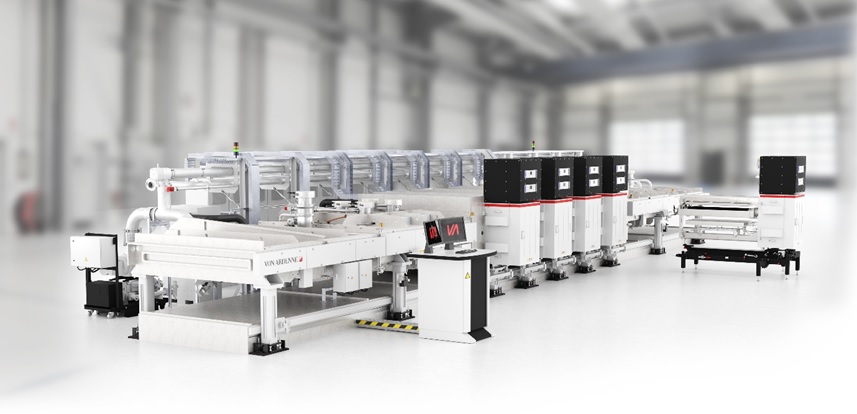
In order to be able to keep up CAPEX- and OPEX-wise with PERC, high-throughput systems are required from the start. Since the HJT technology is still relatively new at GW scale, our customers expect further developments and optimizations in the process flow in the coming years. Also, this is taken into account in the design of our XEA|nova L platform to the extent that you can change the PVD sequence without great effort. For example, you can do sputter up and sputter down processes without vacuum break in any order or apply seed and bulk layers with different physical properties. And all of this with gross throughputs of 10,000wph and higher.”
Getting production line throughputs maximized for n-type cell lines is now being prioritized in the industry. What benefits will n-type manufacturers see in using these tools?
Dr. Sebastian Gatz: “Throughput and uptime of the individual systems are one of the decisive factors for a positive overall CoO. In addition, the HJT process sequence is shorter than with the one for TOPCon PERC. Of course, this only applies if all 6 process steps for HJT are on the same level as the fully optimized PERC steps. Between 10 and 12 process steps are required for double-sided TOPCon cells. In addition to the increased efforts of integration, the increased need on automation for each equipment can also come at the expense of production yield. Of course, this only applies if all 6 process steps for HJT are on the same level as the fully optimized PERC steps. But here we are right now and that is the reason why so many are evaluating the HJT technology seriously in pilot production or already investing in GW production.”
There is now growing interest in heterojunction, both within China and elsewhere globally. Is equipment standarization any closer, compared to a few years ago?
“The question here is what is meant by standardization. GW solar cell production expansions are done via clustering of several systems directly next to one another. It is important that the interfaces of the process systems are aligned with those of the automation supplier. Other than that, the specifications come more from the wafer formats. While we were still assuming M6 as the dominant format six months ago, the compatibility of our systems with other wafer formats such as M10 or G12 are requested and those requirements can be met with our systems. In addition, there has recently been an increased demand to be able to process half-cut cells too. The nice thing about the HJT process sequence is the fact that all these potential changes in wafer format can be applied on the 6 different process steps. Things look different for PERC, where new wafer formats mean major modifications or even new investments in the process chain.”
Looking a few years out, and assuming n-type production starts to take significant market-share from p-type, where are the areas for further optimization?
“For sure that is the process sequence itself. Once the production for HJT has really reached GW scale mass production, the swarm of process experts will be able to turn all nodes and the supply chain will have adjusted to the increased demand, the efficiency will increase continuously and the manufacturing costs will decrease further. An essential step is reducing the relative cost of TCO in the cell in terms of cents/W, which can be reached by process optimization, alternative materials, target orders in GW scale, and highest throughputs in each individual PVD.
And then we can see tandem technology approaching us on the horizon. Regardless of whether used on HJT or PERC, this is the next step on how to increase the efficiency in the module. This is still on the R&D and pilot line scale, but the progress is already considerable. Our customers want to get a grip on challenges such as scalability and stability in 2 stages: single wafer processes in a R&D cluster-type system or inline pilot systems. Once the right process chain has been found, we will scale the technology to GW equipment.”
Von Ardenne is delivering a keynote talk at PV CellTech 2020 Online on 28 October. What are the key topics that will be discussed further during the presentation?
“First of all we are very pleased that, despite these challenging times, you managed to organize this top-class event with that outstanding lineup. We appreciate to report on the latest developments from vacuum equipment point of view. This year there is a strong focus on our XEA|nova equipment for the HJT market, reporting above 24% efficiencies with 750mV open-circuit voltages in production. The XEA|nova L platform with throughputs of 10,000wph+ and why we think it is the answer to some of the above-mentioned challenges for HJT are discussed further. At the end we want to provide also an overview about our R&D and pilot system solutions for the tandem technology approach.”
Dr. Sebastian Gatz will be delivering a keynote presentation at PV CellTech 2020 Online, titled ‘10,000 wafer per hour sputtering for cost-effective GW cell production’, during Session 1 on Day 2 of the event (28 October 2020). To learn more about the full agenda, or to register to attend the full event online this year, please follow the tabs at the link here.

")


