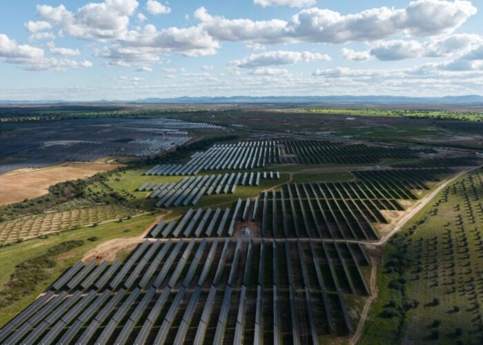
A triple-junction thin-film silicon cell structure that utilizes the majority of the solar spectrum is in development phase at Mitsubishi Electric. A 5mm x 5mm cell is claimed to have produced conversion efficiencies of 14.8% in the lab. High-quality film-deposition processing of each layer was required. Mitsubishi said that first layer absorbs short wavelengths and the third layer absorbs long wavelengths. Texture fabrication was also applied to transparent electrodes for optimal confinement of light.
Mitsubishi said it intends to continue its R&D of the triple-junction cell with the aim to raise conversion efficiencies further. Work will focus on improving cell structure and materials as well as processing conditions.
This article requires Premium SubscriptionBasic (FREE) Subscription
Unlock unlimited access for 12 whole months of distinctive global analysis
Photovoltaics International is now included.
Already a subscriber? Sign In
- Regular insight and analysis of the industry’s biggest developments
- In-depth interviews with the industry’s leading figures
- Unlimited digital access to the PV Tech Power journal catalogue
- Unlimited digital access to the Photovoltaics International journal catalogue
- Access to more than 1,000 technical papers
- Discounts on Solar Media’s portfolio of events, in-person and virtual

