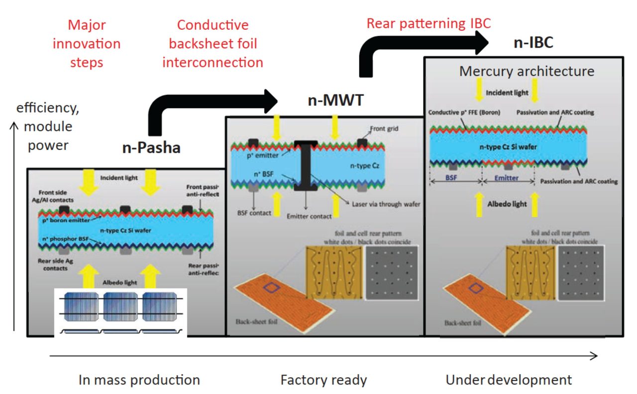
Photovoltaics International Papers

Premium
Materials, Photovoltaics International Papers
Solar cell performance depends on material quality, as well as on the architecture of the cell. In the search for higher-performing cells, an ability to visualize the bulk and surface quality of the material is an advantage; to do this non-destructively, even in-line, is even better. It would be good to have X-ray vision to look inside, would it not? X-ray diffraction imaging (XRDI) does just that. Images are obtained of the distortions caused by crystal defects, and quantitative measures of the lattice deformation are available. In this paper the results obtained on a commercially available XRDI tool are compared with those from a largescale public research facility.
Premium
Cell Processing, Photovoltaics International Papers
Actual solar cells are large-area, two-dimensional (2D) devices with lateral variations in internal voltage, but most of the time they are represented by simplistic equivalent circuits consisting of a few lumped elements. Griddler© is a finite-element-method (FEM) simulator that constructs and solves the full 2D distributed network representation of a metallized solar cell. Not only is this approach far more versatile and adaptable to real-world problems, accurate in predicting subtle device characteristics, and compatible with mapping data, but it can also be implemented in a way that is as easy and quick to use as a handy calculator. This paper covers a broad range of applications related to full-area 2D modelling and introduces Griddler 1.0 - a compact freeware computer program that places much of that power at the fingertips of any solar cell engineer with a PC.
Premium
Fab & Facilities, Photovoltaics International Papers
The latest rounds of formal complaints against alleged breaches of trade agreements, the initiation of circumvention investigations, and preliminary announcements and rulings in various countries and trading zones all demonstrate that the multidimensional trade conflict in global PV markets is far from being resolved and is still simmering. The trade dispute is largely focused on the import of downstream products (c-Si wafer, cell and module) in current and prospective high-volume markets, such as the EU, the USA and potentially India. These nations or trading zones have implemented, or have proposed to implement, anti-dumping and countervailing duties, predominantly targeted against Chinese downstream producers. New rounds of investigations might lead to existing tariffs being extended to Taiwanese manufacturers that directly or indirectly import into the USA, while the EU might scrap a previous quota and minimum price system and revert to tariffs. This paper gives a brief historical review of the global PV trade dispute, and analyses the formal and legal grounding of anticircumvention actions, which in general increase the complexities of business planning. Because more than 70% of the global downstream manufacturing capacity is located in China and Taiwan, the manufacturers in these regions have no choice but to embrace an internationalization strategy that consists of production offshoring. The paper concludes with the introduction of potential strategies and recommendations which take account of increased complexities and uncertainties in business planning that arise from shifting trade barriers.
Premium
Photovoltaics International Papers, Thin Film
For some years CIGS was seen as the great white hope of the PV industry, until c-Si revealed its true competitiveness in mass production. Most companies dedicated to the commercialization of CIGS, many of which were VC financed, did not survive this development. Nonetheless, the industry has recently seen new corporate entrants with impressive plans for the roll-out of CIGS. The motives for these strategic actions are of interest, so a cost-of-ownership calculation was performed for a state-of-the-art CIGS production: the result is that current production cost for a CIGS module is €0.44/Wp, with material and depreciation being the main cost drivers. Although significant progress has been made in the last few years, this is still higher than the production costs for standard c-Si modules. However, the costs for CIGS coating materials, which correspond to the wafer in a c-Si module, are significantly lower than those for a wafer. Could this be a motive for the actions that have been witnessed in the CIGS industry? The next task would be to evaluate the further costreduction potential of CIGS and the likelihood of its realization.
Premium
Photovoltaics International Papers, PV Modules
The potential for PV modules to fail before the end of their intended service life increases the perceived risk, and therefore the cost, of funding PV installations. While current IEC and UL certification testing standards for PV modules have helped to reduce the risk of early field (infant mortality) failures, they are by themselves insufficient for determining PV module service life. The goal of the Fraunhofer PV Durability Initiative is to establish a baseline PV durability assessment programme. PV modules are rated according to their likelihood of performing reliably over their expected service life. Modules are subjected to accelerated stress testing intended to reach the wear-out regime for a given set of environmental conditions. In parallel with the accelerated tests, modules are subjected to long-term outdoor exposure; the correlation between the accelerated tests and actual operation in the field is an ultimate goal of the programme. As understanding of PV module durability grows, the test protocols will be revised as necessary. The regular publication of durability ratings for leading PV modules will enable PV system developers and financiers to make informed deployment decisions. This paper provides summary data for eight module types from the two rounds of testing to date.
Premium
Fab & Facilities, Photovoltaics International Papers
The positive expectations for the global PV market are driven by state-of-the-art PV products which have become economically attractive because of technical optimization. Nonetheless, scientists and engineers face the next generation of wafer-based PV technologies in terms of processing recipes and automation techniques. In this paper, motivations, challenges and advances relating to the handling of ultrathin PV substrates are identified for future application. A brief look out of the PV box at neighbouring disciplines in high-tech sectors will also be taken. The differences and advances in the automated handling of ultrathin substrates will be highlighted as well as the difficulties for transportation. The advanced production challenges of a gripperbased substrate movement will be accompanied by increased cleanliness requirements, as test results from the Fraunhofer IPA automation lab show.
Premium
Cell Processing, Photovoltaics International Papers
The combination of metal-wrap-through technology with a unit cell design, referred to as AP-MWT architecture, is proposed for the purpose of operating under low and concentrated irradiance. On the illuminated side, the negative polarity is electrically separated by using an emitter window surrounding the perimeter of each unit cell. The final functioning silicon-based device consists of an arbitrary amount of unit cells with perimeter dimensions ranging from 1cm x 2.25cm to 14cm x 13.5cm. The Czochralski-based bulk material, as well as the assembly approach, conforms with state-of-the-art industrially feasible technologies. For irradiances corresponding to 1 and 10 suns, median efficiencies of 19.8% and 20.9% and top efficiencies of 20.2% and 21.0% have been achieved. Thanks to the flexibility in size, interconnection and irradiance, awide range of current-voltage ratios are covered, providing customized solutions beyond the conventional flat-panel market.
Premium
Photovoltaics International Papers, Power Generation
As PV systems proliferate and become an important part of the global energy mix, it is increasingly important to forecast their energy output in order to ensure a safe and reliable integration of their variable output into electric power grids. One of the main prerequisites for that is the detailed recording and interpolation of the actual irradiance in a spatially resolved way. Such 2D irradiance maps would also allow the assessment of the performance of the many PV systems that do not have irradiance sensors installed at the site. The maps are ideally based on a dense network of irradiance sensors; however, in many cases the costs of high-precision pyranometers, real-time monitoring and frequent maintenance are prohibitive for such operational forecasting systems. On the other hand, many PV installations are in fact equipped with reference cells in the plane of array (POA) for evaluating and monitoring the performance of the systems. Adding this network of reference cells to existing pyranometer networks (from meteorological services or research institutes) would substantially help in improving the accuracy of the irradiance maps. This paper introduces an irradiance conversion technique that allows POA irradiance measurements from an on-site reference cell to be converted to global horizontal irradiance data, which can then collectively be used to generate large-area irradiance maps.
Premium
Fab & Facilities, Photovoltaics International Papers
Two years of overcapacity in the global PV supply chain have led to investment in new manufacturing capacity grinding to a halt. However, booming global end-market demand has brought the supply–demand imbalance under control and as a result the world’s leading equipment suppliers have begun looking at serious capacity expenditure. On the basis of recent announcements and annual report publications by some of the leading manufacturers, this article examines where, when and by whom capacity expansions are now planned.
Premium
Cell Processing, Photovoltaics International Papers
The n-Pasha n-type silicon solar cell currently achieves an average conversion efficiency of 20.2% using a relatively simple process flow. This bifacial cell concept developed by ECN is based on homogeneously doped p+ front and n+ back surfaces. To enhance the cell efficiency, it is important to reduce the carrier recombination within the boron-diffused p+ region and at its surface. This paper addresses a novel way to tune the boron-doping profile and presents advanced surface passivation schemes. In particular, it is demonstrated that a very thin (2nm) Al2O3 interlayer improves the passivation of the boron-doped surface; the Al2O3 films were deposited in industrial atomic layer deposition (ALD) reactors (batch or spatial). Moreover, it is shown that the boron-doping profile can be improved by etching back the boron diffusion. On the basis of the results presented, it is expect that n-Pasha solar cells with 21% efficiency will soon be within reach.

Subscribe to Newsletter

Upcoming Events

Media Partners, Solar Media Events
September 2, 2025
Mexico City, Mexico
Solar Media Events
September 16, 2025
Athens, Greece
Solar Media Events
September 22, 2025
Bilbao, Spain
Solar Media Events
September 30, 2025
Seattle, USA
Solar Media Events
October 1, 2025
London, UK