Thin Film

Premium
Photovoltaics International Papers, Thin Film
Because of its attractive electronic and optical properties, zinc oxide (ZnO) has found widespread use as a front and back electrode in commercial solar cells. ZnO can be deposited on glass using a variety of different methods, of which vacuum-based techniques are the most commonly used in industrial applications. Aluminium-doped sputtered ZnO:Al (AZO) has been studied intensively for use as a front contact in a-Si/μc-Si tandem cells. The implementation of AZO in series production has been hindered by reproducibility issues stemming from the combination of deposition and subsequent etching steps that are necessary to tune the ‘haze’ of the layers for optimal light scattering. Boron-doped ZnO:B (BZO), deposited by low-pressure chemical vapour deposition (LPCVD), has become a cost-effective option for module manufacturers, since the desired layer morphology can be produced as grown without the need of post-growth chemical etching. This paper addresses the different aspects of using AZO and BZO layers as front contacts for a-Si/μc-Si tandem modules fabricated in series production. The properties of the underlying ZnO layers put restrictions on the layer properties and process parameters that are used in the deposition of a-Si and μc-Si.
Premium
Photovoltaics International Papers, Thin Film
In situ, real-time and off-line polarization spectroscopies have been applied in studies of large-area spatial uniformity of the components of multilayer stacks in hydrogenated silicon (Si:H) and cadmium telluride (CdTe) thin-film photovoltaic (PV) technologies. Such reflection spectroscopies involve first the measurement of spectra in the reflected-to-incident polarization state ratio of the light wave (or the ellipsometry angles of the reflecting multilayer stack), and then the analysis of these spectra to determine the thicknesses and properties of component layers of the stack. In addition, expanded capabilities result from measurement/analysis of the irradiance ratio and the degree of polarization of the reflected beam, simultaneously with the polarization state ratio, particularly for rough surfaces with in-plane roughness scales of the order of the optical wavelength or greater that scatter and depolarize the light beam. This paper provides examples of 1) real-time monitoring of texture etching of the transparent conducting oxide ZnO:Al; 2) real-time monitoring and off-line mapping of roll-to-roll deposited hydrogenated amorphous silicon (a-Si:H); and 3) large-area mapping of coated glass panels used in low-cost CdTe PV technology. For a-Si:H and CdTe thin-film PV technologies, the focus is on the characterization of the window layers, which are p-type protocrystalline Si:H and n-type cadmium sulphide (CdS), respectively. Analysis of the thickness, phase and structure of the window layer material over the area of the PV panel is critical in order to design processes for uniformity of high performance. Descriptions are given of future directions in novel instrumentation development that will enable mapping for uniformity evaluation at the high speeds required for on-line analysis.
Premium
Photovoltaics International Papers, Thin Film
Transparent conductive oxides (TCOs), such as aluminium-doped zinc oxide (ZnO:Al), play an important role in thin-film photovoltaics. As a material for front contacts, ZnO:Al is standard in industrial-scale production, especially in the field of Cu(In,Ga)Se2 solar cells. Over the last few years, there has been a strong push to use ZnO:Al films on glass as substrates for amorphous or amorphous/microcrystalline silicon solar cells, and these films have now been introduced as an alternative to the typically used fluorine-doped tin oxide (SnO2:F) films in production. Sputtering coaters for large area deposition of ZnO:Al are widely available, and ZnO:Al films are produced in these coaters by sputtering of ceramic targets. This technology offers high process stability and is therefore favoured over reactive sputtering of metallic targets. With respect to cost and quality, however, the reactive process is an interesting alternative. In this paper we will give an overview of the process of reactive sputtering of ZnO:Al and discuss the most important insights.
Premium
Photovoltaics International Papers, Thin Film
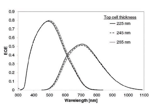
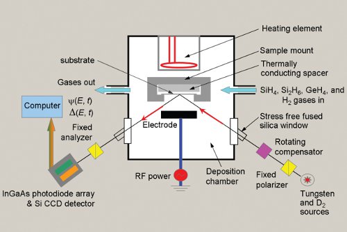
Optical probes based on polarized light spectroscopy, including spectroscopic ellipsometry (SE) and polarimetry, have been applied in research and process development for the three major thin-film photovoltaics technologies, including thin-film hydrogenated silicon (Si:H), cadmium telluride (CdTe), and copper indium-gallium diselenide (CuIn1−xGaxSe2). Real-time SE during materials fabrication has provided insights into the nucleation, coalescence, and structural evolution of these thin films. These insights have led, in turn, to guiding principles for PV performance optimization, as well as future directions for real-time process control. The optical properties deduced simultaneously with the layer thicknesses using real-time SE have been applied to characterize the phase composition of materials (amorphous versus crystalline), the mean free path and grain size, and the relative free carrier concentration. As a result, analytical formulae for the optical properties of PV materials have been developed with free parameters that are linked to basic materials properties. This paper shows how the formulae and associated parameter-property relationships can serve as a database for analyzing complete PV stacks, with future prospects for mapping layer thicknesses and basic materials properties in on-line monitoring applications for large-area PV plates and modules.
Premium
Photovoltaics International Papers, Thin Film
A growing number of thin-film photovoltaic module producers are either trying to keep up with the current cost leader or aiming to differentiate on product design. Calyxo is dedicated to both keeping the pace in the US$0.50/Wp race and introducing new product generations, therefore delivering more value to the customer. We have tried to improve the methodology and approaches for knowledge building in the individual process steps, by learning the relevant interactions between them, as well as ramping volume and lowering manufacturing cost in the first production line. Developing and building the deposition equipment suited to the high process temperatures of approximately 1000°C at atmospheric pressure took some time, but the technology itself now enables Calyxo to benefit from significant cost savings both on capital investment and operational cost – compared to some well-known vacuum deposition methods. Besides the continuous decrease in manufacturing costs, even early on in building the manufacturing capacity, the ability to design the product itself according to the needs of the customers proved itself to be a decisive factor in ensuring competitiveness. This paper aims to give an insight into some of the basic design features of a new product generation and how the so-called new CX3 product will generate more watts by improved performance: delivering better customer value by decreased voltage to save on BOS costs and ensuring further increased field durability through an optimized package design.
Premium
Photovoltaics International Papers, Thin Film
Conversion efficiencies of thin-film silicon solar cells can be increased by nanotexturing of the cells. This nanotexturing step allows for a larger fraction of the incoming light to scatter and diffract, so that both the total absorption of light in the solar cell and the short circuit current is enhanced. In this study, we investigate the optics of thin-film silicon solar cells by numerically simulating Maxwell’s equations by a finite-difference time-domain algorithm. Starting with periodically textured solar cells, the influence of the texture period and height on the quantum efficiency and short circuit current were investigated. With this understanding of the optimized surface texture for periodically textured solar cells, the possibility of interpreting the optics of randomly textured solar cells will be discussed.
Premium
Photovoltaics International Papers, Thin Film
As recently as a couple of years ago, solar panels based on thin-film manufacturing technology were being promoted as the low-cost alternative to crystalline silicon. Not only was it cheaper, but thin film also had a convincing roadmap which guaranteed this cost advantage for the foreseeable future. That was 2008, when persistently high polysilicon prices seemed inevitable as demand for solar electricity boomed. We now know that assumption to be false, and although we all knew polysilicon prices would fall eventually, no one predicted the speed and magnitude with which they crashed: in the space of several months, prices reached the point where any advantage associated with the lower materials costs of thin-film manufacturing were completely blown away.
Premium
Photovoltaics International Papers, Thin Film
The three most viable thin-film photovoltaic technologies – cadmium telluride (CdTe), copper-indium gallium (di)selenide (CIGS), and amorphous silicon (a-Si) – continue to mature and grow technologically and in market stature. But apart from the dominance shown by CdTe leader First Solar, the rest of the TFPV manufacturers have had a fairly difficult time making significant commercial inroads as the price of mainstream crystalline-silicon modules plummeted over the past couple of years. Other factors delaying the long-predicted age of thin film include bankability challenges and difficulties in reducing production and system costs. Yet entrants in all three thin-film categories have reason for optimism, as they push toward a competitive market position. This paper provides an overview of the current status of the thin-film PV sector and its players, offering insights into why certain companies might emerge successfully in the years ahead.
Premium
Photovoltaics International Papers, Thin Film
Magnetron-sputtered ZnO:Al is often used as a front contact in thin film silicon solar cells due to its transparent conductive oxide (TCO) properties that allow texturization by chemical etch processes to introduce light trapping. The transparency, conductivity, and surface texture after etching depend strongly on the sputtering conditions. Consequently, the typical preparation method is to find the right balance in TCO properties and light scattering, leading to a very narrow sputtering parameter window. It is preferable to separate the electro optical optimization from that of texturization to allow for a larger process window and improve ZnO:Al film properties further. This paper presents some methods of controlling the surface features using various mixtures of two step etching processes in aqueous solutions of HF and HCl. Results include methods for controlling the density of craters, texturizing compact ZnO:Al films, and fabricating novel modulated surfaces with more than one characteristic feature size. The two step etch process enables the creation of good surface textures even on high rate material that, via state of the art HCl etching, tend to lead to poor solar cell performance.
Premium
Photovoltaics International Papers, Thin Film
Highly conductive transparent films are of significant interest in the field of thin-film photovoltaics. The solar cell type defines the necessary properties of the TCO used, as, besides the obvious qualities of transparency and conductivity, stability and morphology are important. The most significant properties of these aspects for front contacts in amorphous/microcrystalline silicon tandem, CIGS and CdTe solar cells are presented in this paper. Commonly used deposition techniques like CVD and sputter technology are described herein, focusing on particular techniques like SnO2:F and ZnO:B (CVD) and ZnO:Al (sputtering). New developments of deposition methods are also discussed.

Subscribe to Newsletter

Upcoming Events

Solar Media Events
May 1, 2024
Dallas, Texas
Solar Media Events
May 21, 2024
Sydney, Australia
Solar Media Events
May 21, 2024
Napa, USA