Thin Film

Premium
Photovoltaics International Papers, Thin Film
This is the second part of a review article series about current topics in R&D concerning Cu(In,Ga)(Se,S)2 – or CIGS – solar cells. In the first part, which appeared in the previous edition of Photovoltaics International, the focus was on CIGS absorber layer formation. This second part will discuss another essential part of CIGS solar cells – the buffer layer – in conjunction with metastabilities in these types of cell.
Premium
Photovoltaics International Papers, Thin Film
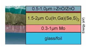
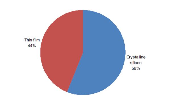
Since the demonstration of the first CuInSe2 solar cell in 1974 by scientists at Bell Laboratories, a lot of effort has been put into the development of cost-effective processes for highly efficient Cu(In,Ga)(Se,S)2 – or CIGS – solar cell devices. In 2012 these efforts led to the first gigawatt CIGS solar module production facility operated by Solar Frontier, a company that has a long history in R&D and originates from ARCO Solar, who developed the first commercial CIGS solar modules at the beginning of the 1990s. However, several start-up companies employing CIGS technology are presently struggling in the currently harsh market environment. Even though world-record laboratory solar cells now demonstrate 20.3% efficiency using a three-stage co-evaporation process, and full-size modules achieve 14.6% employing a similar method, efforts in research and development are more important than ever in order to increase cell efficiency, to bridge the gap between cell and module efficiencies, and to develop cost-effective and robust manufacturing processes. This paper gives an overview of current research topics under investigation by research institutes and industry, with a main focus on CIGS absorber formation. Along with other research results published by groups all over the world, this paper covers recent research results obtained at the Helmholtz-Zentrum Berlin für Materialien und Energie (HZB) and briefly mentions the work of the Photovoltaic Competence Center Berlin (PVcomB), a joint initiative of the Technical University of Berlin (TU Berlin) and HZB.
Premium
Photovoltaics International Papers, Thin Film
Thin-film PV modules are one of the most sustainable options for the generation of electricity, with low material consumption and short energy-payback times. Both of these factors are essential for paving the way towards a terawatt PV market. However, the cost-competitive production of PV modules has become extremely difficult, and module producers are facing huge challenges. A rapid technology transfer from research to industry is therefore required in order to introduce innovations for lower production costs and higher conversion efficiencies. At the Competence Centre Thin-Film- and Nanotechnology for Photovoltaics Berlin (PVcomB), founded by the Helmholtz-Zentrum Berlin (HZB) and the Technical University Berlin, two R&D lines for 30 x 30cm2 modules based on thin-film silicon and copper indium gallium (di)selenide (CIGS) respectively are operated. Robust baseline processes on a high efficiency level, combined with advanced process and device analytics, have been established as a basis for the introduction and development of further innovative technology steps, and their transfer to industry.
Premium
Photovoltaics International Papers, Thin Film
Thin-film solar cells (TFSCs) still hold unlocked potential for achieving both high efficiency and low manufacturing costs. The formation of integrated interconnects is a useful way of maintaining high efficiency in small-scale solar cells by their connection in series to form a module. Laser scribing is widely used for scribing a-Si- and CdTe-based TFSCs to form interconnects. The optical properties of the ternary copper-indium-gallium (di)selenide (CIGS) compound are well suited to the solar spectrum, with the potential to achieve a high photoelectrical efficiency. However, since it is a thermally sensitive material, new approaches for the laser-scribing process are required, to eliminate any remaining heating effects. For flexible CIGS solar cells on non-transparent substrates (metal foils or polymer), the scribing process faces additional challenges. This is one reason why ultrashort laser pulses yield better results in terms of scribing quality and selectivity. The modelling of laser energy coupling and an extensive characterization of laser scribes allow approaches to be developed for laser scribing of CIGS solar cells on flexible polymer substrates. The measured high efficiency of the resulting high-speed laser-scribed, integrated CIGS mini-modules proved the capability of this approach.
Premium
Photovoltaics International Papers, Thin Film
This paper presents Calyxo’s recent advances in product design that have resulted in independently confirmed peak aperture-area efficiencies of 13.4% for modules and 16.2% for cells. Some insight is given into a suitable product design for achieving the highest reliability possible, even in hot climates such as Australia, with no signs of degradation during the first three years of deployment in the field. These technical advances and the midterm production-cost target of US$0.50/Wp allow a forecast levelized cost of electricity (LCOE) of under US$0.10/KWh, especially in sunny regions of the world.
Premium
Photovoltaics International Papers, Thin Film
Lifetime guarantees of more than 20 years are a target for the long-term stability of solar modules. An important point for the future of CIGS solar cells is to understand the impact of metastable behaviour on long-term stability. Accelerated ageing under open-circuit conditions leads to a drop in open-circuit voltage (Voc). A decrease in the net doping density is responsible for the drop in Voc and consequently the drop in the photoluminescence (PL). In the initial state the electroluminescence (EL) ideality factor exhibits a value close to unity, as expected from theory. After the dark anneal an increase in the EL ideality factor is observed, and an EL measurement at constant voltage shows a decrease in EL: both these behaviours are due to a pile-up of negative charges at the heterointerface. The application of a positive bias or an illumination during the endurance test leads to an optimization of stability. This paper shows that PL and EL can distinguish between bulk and interface properties and are well suited for the detection of degradation mechanisms.
Premium
Photovoltaics International Papers, Thin Film
Advances in nanofabrication for enhancing the efficiency of optical devices, such as solar cells and photo-detectors, via nanostructuring have attracted a great deal of interest. A photoconversion strategy employing nanorods (NRs) has emerged as a powerful way of overcoming the limitations of planar wafer-based or thin-film solar cells. But there is also a broad spectrum of challenges to be tackled when it comes to putting into practice cost-effective NR solar cell concepts. ROD-SOL is a 10-partner, ‘nanotechnology for energy’ project with end-users, equipment manufacturers and institutes from six countries forming the consortium. The aim of the project is to provide the photovoltaic market with a highly efficient (> 10%), potentially low-cost, thin-film solar cell concept on glass, based on silicon nanorods. This paper presents the project’s achievements and discusses what the future might hold for nanotech-based solar energy production.
Premium
Photovoltaics International Papers, Thin Film
Today, crystalline-Si photovoltaics (PV) dominate the market, accounting for more than 85% of market share in 2010. A large scientific community made up of academic as well as industrial stakeholders strives to find solutions to improve device efficiencies and to drive down costs. One of the important cost elements of a module is the c-Si wafer itself. This paper discusses the fabrication of a carpet of c-Si foils on glass, either by layer transfer of an epitaxially-grown layer or by bonding of a very thin wafer, and processing this c-Si thin-foil device into a photovoltaic module. This could constitute an advantageous meet-in-the-middle strategy that benefits not only from c-Si material quality but also from thin-film processing developments.
Premium
Photovoltaics International Papers, Thin Film
Sales of critical subsystems used in thin-film PV manufacturing equipment are expected to reach $324M in 2011, and the outlook is for this figure to grow by 3.74% in 2012 to $336M. This expectation is going against the trend for the industry as a whole, which is predicted to decline next year as revenues from cell and module manufacturing weaken. The reason for this countermovement is the opportunities available to manufacturers who are willing to invest in the latest thin-film PV equipment to drive down costs and force unprofitable competitors out of business. While the same opportunities exist for crystalline silicon manufacturing, the number of well-resourced companies signalling their intention to invest in thin-film technologies should ensure a positive year for suppliers of equipment and critical subsystems to this segment of the industry.
Premium
Photovoltaics International Papers, Thin Film
In terms of material properties, plasma-enhanced chemical vapour deposition (PECVD) of ZnO has advantages over sputtering techniques, due to the variety of available precursors, and the different dopants for achieving certain levels of n-type and, controversially discussed, p-type transparent conductive oxides (TCOs) on various substrate materials. This paper considers the deposition of boron-doped zinc oxide for n-type TCO-application on substrates of dimensions up to 50×50cm2 and at a temperature range of 50 to 450°C using a PECVD reactor with a plasma frequency of 13.56MHz. The materials’ characteristics such as transparency, carrier concentration and structural properties are discussed as a function of the deposition parameters. The deposition temperature strongly affects the crystallographic and morphological appearance of the deposited thin films, which was investigated using field emission scanning electron microscope (FESEM) and X-ray diffraction (XRD) methods. The electronic band structure-dependent characteristics were studied using ultraviolet-visible (UV-vis) spectroscopy and Hall measurements. Secondary ion mass spectrometry (SIMS) measurements complete the characterization methods for qualitatively verifying the incorporation of dopants and impurities. Results are reported for columnar-grown boron-doped ZnO with optical transparency greater than 80% in the visible range and a maximum carrier concentration of 1020cm-3.

Subscribe to Newsletter

Upcoming Events

Solar Media Events
April 10, 2024
Dallas, Texas USA
Solar Media Events
April 17, 2024
Lisbon, Portugal
Solar Media Events
May 1, 2024
Dallas, Texas
Solar Media Events
May 21, 2024
Napa, USA