Thin Film

Premium
Photovoltaics International Papers, Thin Film
With the never-ending need to reduce production costs, interest in atmospheric deposition techniques is steadily increasing. Even though atmospheric deposition is not new to photovoltaics, and in some cases is actually required to get the best cell performance, many of the fabrication processes for photovoltaic cells are vacuum-based. Due to the diversity in atmospheric deposition techniques available, there are opportunities for applications in thin film and patterned deposition. This paper discusses some of the deposition techniques and their applications, benefits and drawbacks.
Premium
Photovoltaics International Papers, Thin Film
This paper presents fluorescence detection as a new tool for the investigation of the degradation of EVA. The superior sensitivity of the setup contained herein allows an early assessment of the changes of the EVA after only 20 hours of damp-heat exposure. A newly developed scanning system allows the spatially resolved inspection of entire PV modules. Degradation of the encapsulants was detected after two years’ outdoor exposure, as was the effect of cracks in c-Si cells, which coincide well with cracks made visible by electroluminescence.
Premium
Photovoltaics International Papers, Thin Film
Thin-film solar photovoltaic technology offers the benefits of low-cost and high-volume production. Yet numerous thin-film PV startups have struggled in their efforts to commercialize complex, expensive production technologies, as production ramps have taken longer than expected, and venture capital and other sources of funding have run dry. This article describes a proprietary cadmium telluride (CdTe) thin-film module production process commercialized by Abound Solar: heated-pocket deposition (HPD) of the semiconductor layer, and the replacement of a traditional lamination process with a novel edge seal. The simple production process has resulted in a fast ramp of module efficiency and throughput. The paper will also describe how the process also results in fast throughput, high yields, and low manufacturing and capital equipment costs.
Premium
Photovoltaics International Papers, Thin Film
Thin-film module production has proven itself as a forerunner in the race to drive down costs for photovoltaics. The type of semiconductor material used is the most differentiating factor for thin-film photovoltaics, playing the decisive role for determining which core processes are employed and what type of equipment is used. This explains why discussions related to thin-film costs and technologies usually focus on the semiconductor type. However, the effects of glass production, processing and handling are often underestimated: factors such as scaling, yield, unit cost and total cost of ownership of the equipment are defined by the glass-production side of the industry. This paper discusses the challenges faced in glass washing and handling in thin-film PV production.
Premium
Photovoltaics International Papers, Thin Film
This paper describes the functionality, applicability, and the development of dependency maps which are the basis for standardized information exchange between responsible parties during the fab design process. Examples and experiences are related to the solar industry; however this generic approach may be applied to a wide range of different industry sectors with similar challenges. The aim is to provide a guideline for realizing a fab design of dynamic and complex production systems. Its main benefit is a higher degree of transparency regarding dependencies within the production system, which results in a reduction of risk for incorrect planning. In addition, it enables the factory designer to execute the fab planning process and further continuous improvements for achieving respective targets.
Premium
Photovoltaics International Papers, Thin Film
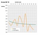
The demand for equipment used to manufacture solar photovoltaic solar cells and modules has grown at an explosive rate over the past five years, and the fastest-growing segment has been for systems used to manufacture thin-film cells and modules. In 2009, demand for this type of equipment reached US$1.9 billion, up from US$0.1 billion in 2004, representing an astonishing 80% compound annual growth rate over the period. However, as with the rest of the industry, 2009 saw sales flattened and the business model change from one of rapid growth to that of sustainability. The result of this transition has been some consolidation, with several major equipment vendors strengthening their position through acquisitions. The outlook for 2010 calls for sales of thin-film production equipment to recover and continue growing at a compound annual growth rate of around 15% over the next five years (see Fig. 1).
Premium
Photovoltaics International Papers, Thin Film
It is widely acknowledged that, without government subsidies, solar power still cannot compete effectively with conventional sources of electrical energy. As the industry strives to make solar electricity affordable and as a viable alternative to fossil fuels, solar power technology companies are diligently moving towards reducing the manufacturing cost for solar modules. In the case of thin-film solar cells in particular, as a benchmark, the cost of for solar power must be reduced for it to be competitive or to attain grid parity. This paper presents a number of opinions from industry leaders on how best to decrease this vital cost.
Premium
Photovoltaics International Papers, Thin Film
The recent photovoltaic industry shakeout which started around Q3 2008 has faced the overcapacity, credit crunch, and economic crisis that significantly declined the average selling price by 50 - 65%, including the price of thin-film photovoltaic modules. The changing business environment has put significant pressure on all PV manufacturing technologies but more candidly on amorphous silicon thin-film single-junction module manufacturers to advance and scale up the device efficiency and aggressively drive cost reduction. This paper outlines the approach taken at Moser Baer Photovoltaic Technologies India Limited (PVTIL), including process optimization and device management strategies, to enhance the module efficiency (total area) of the single-junction amorphous silicon quarter size, 1.43m2, substrate as manufactured using Applied Materials’ SunFab line.
Premium
Photovoltaics International Papers, Thin Film
Chemical stoichiometry along with depth profiling and metallic contamination is of considerable interest for photovoltaic thin films. Conversion efficiency can be affected for example if primary components, e.g. Cd and Te, are not present at proper ratios. Moreover, amorphous silicon can vary substantially between sources and deposition technique, and qualitative comparison of trace metallic contaminants may not be sufficient to ensure final thin-film quality. This discussion presents data from atomic emission and mass spectrometry techniques that quantitatively and accurately describe both bulk and trace elemental compositions in photovoltaic materials, various thin-film matrices, and the final thin-film cell and module.
Premium
Photovoltaics International Papers, Thin Film
Highly conductive transparent films are of significant interest in the field of thin-film photovoltaics. ZnO-based films in particular have attracted much interest due to the low cost of materials with good film properties for CIGS and a-Si/µc-Si solar modules. Investigations have been ongoing at Fraunhofer IST into ceramic ZnO:Al2O3 targets from different manufacturers. This paper presents a comparison of target material, sputter characteristics and film properties of ZnO:Al. Sputter characteristics are in this case determined by voltage and current data showing arcing rates at different power loads and process pressures. ZnO:Al films are deposited by DC magnetron sputtering with various deposition parameters (e.g oxygen flow, total pressure, sputtering power and substrate temperature) and investigated with respect to optical and electrical properties. A correlation between film properties, sputter characteristics and target material can therefore be determined. As it appears that arcing has the biggest influence on film properties, the ceramic target material can be optimized for minimal arcing.

Subscribe to Newsletter

Upcoming Events

Solar Media Events
May 1, 2024
Dallas, Texas
Solar Media Events
May 21, 2024
Sydney, Australia