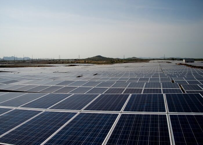
Anwell Technologies has produced its first a-Si thin-film solar panel at its 40MW solar plant in Henan, China using in-house technology.
“When Premier Wen Jiabao visited us in July 2008 and tasked us to address China’s need for power saving and next generation energy infrastructure, we knew we couldn’t let China down. True to our ethos of making the impossible possible, we have produced our first a-Si thin-film solar panel,” said Franky Fan, the Chairman & CEO.
Try Premium for just $1
- Full premium access for the first month at only $1
- Converts to an annual rate after 30 days unless cancelled
- Cancel anytime during the trial period
Premium Benefits
- Expert industry analysis and interviews
- Digital access to PV Tech Power journal
- Exclusive event discounts
Or get the full Premium subscription right away
Or continue reading this article for free
The equipment used was built from scratch using Anwell’s proprietary technologies for the key production processes of a-Si thin-film solar panel including Plasma-enhanced chemical vapor deposition (PECVD), sputtering, laser scribe and transportation system. Using in-house technology will enable the group to have a cost-saving advantage through its vertically integrated model over other solar panel producers who have to import their own equipment.
Anwell’s PECVD system is the world’s first multi-substrate-multi-chamber deposition tool boasting higher productivity and lower manufacturing cost for 1.1 by 1.4m a-Si thin-film solar panel with its unique and innovative batch and cluster design.
The next step for the group is to optomize the production process for mass production. Concurrently Anwell has began R&D on new equipment that will increase their production capacity to 120MW by the end of 2010.


