The production of crystalline Silicon (c-Si) solar cells and thin-film modules has moved from a small quantity niche product to global volume markets and mass production scale. A review of the evolution in process technology of this young industry reveals laser processing to have played an ambiguous role in the last 15 years.
The first process step suitable for laser processing was via drilling for Metal/Emitter Wrap Through (MWT/EWT) solar cells, which however could only reach a limited market volume as MWT/EWT never took off to become a mainstream solar cell technology.
Try Premium for just $1
- Full premium access for the first month at only $1
- Converts to an annual rate after 30 days unless cancelled
- Cancel anytime during the trial period
Premium Benefits
- Expert industry analysis and interviews
- Digital access to PV Tech Power journal
- Exclusive event discounts
Or get the full Premium subscription right away
Or continue reading this article for free
The second one was the laser edge isolation (LEI) process, which became the leading technology to isolate the front and rear sides of the industrial standard c-Si solar cells. Only a few years later it was gradually replaced by a single sided wet chemical etching process yielding higher cell efficiencies.
In parallel to the laser processes for c-Si solar cells, laser scribing technologies (P1, P2, and P3 patterning) for thin-film solar modules were developed and introduced to the market, but limited by the smaller market share of the thin-film compared to the c-Si technology.
From 2005, work on new technologies for standard c-Si solar cells like laser-doped selective emitter (LDSE) and laser contact opening (LCO) started. LDSE became another short hype around the year 2010 and was superseded by a continuously optimized printing technology rendering the benefits of a selective emitter unnecessary. We have therefore seen a lot of up and downs for laser processing in the PV industry over more than a decade.
Today it looks like LCO is about to establish itself as a mainstream process in the manufacturing of industrial standard solar cells. The reason can easily be found in the international technology roadmap for PV (ITRPV).
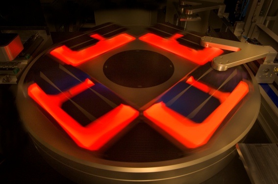
According to the ITRPV the passivated emitter rear cell (PERC) is becoming a dominating technology in the area of c-Si solar cells during this and the next two years wherein LCO is a necessary process step. So far there is no suitable metal paste to be fired through the deposited passivation layer. Consequently, laser ablation is the most cost effective method to locally open the area to be contacted by the fully covering Aluminum paste on the rear side of the solar cell.
Next-generation ITRPV technologies indicate that the front side dielectric (usually SiN) can be opened by lasers as well to enable direct plating on Silicon (PoSi). As long as the Cu plating technology is lacking the ability to provide the inevitable diffusion barrier between Cu and the Si wafer, the PoSi technology is the main road to replace the costly Ag metal grid with the much cheaper Cu, since it can plate a stack of Ni, Cu, and Ag or Sn, which is required to embed Cu in between a diffusion inhibiting and a surface passivating layer.
Going one more step further into the next-generation ITRPV we find again a very promising LCO process, namely in the technology of interdigitated back contact (IBC) solar cells, which are predicted to enable the jump over 23% efficiency.
Processes and tool solutions for PERC
From a process integration point of view, a line pattern represents the easiest and most common way to implement LCO for PERC. Today, the standard process is a line opening with 30-50µm wide lines, and a line-to-line distance of 1 mm. Such a relatively wide opening in the passivation layer presents a good interface for the subsequent contact formation during the co-firing of the screen printed metal layer.
The larger the local surface opening is the faster and more homogeneously the Aluminum-Silicon alloying process can start. This has a direct influence on the formation of the local back surface field (BSF) during the alloying and affects the final Voc. On the other hand, from the perspective of the PERC solar cell design, the wide opening lines restrict the final cell efficiency, because more open area reduces the passivated area leading to lower current (Isc) and voltage (Voc). In order to extract the whole electrical current from a typical PERC solar cell the required cross-section-equivalent opening ratio is 1% ± 0.2%.
For a line opening pattern, the opening ratio is in the range of 3% to 6%. Increasing of the line to line distance would help to reduce the opening ratio and therefore increase the Voc and Isc, but the series resistance (Rs) and consequently the fill factor (FF) of the solar cell will suffer. Especially for high ohmic wafer material the effect can become dramatic.
It is sometimes believed that an optimum contact design combining the opposing requirements of opening ratio and series resistance would be a dot pattern with equidistant dot-to-dot spacing. The drawback of this design, however, is that contact formation during the co-firing process is made difficult.
While a line represents a one-dimensional opening which allows for compensating local inhomogeneity of the local BSF (e.g. voids), every dot is a single event which contributes significantly to the final cell performance. If the contact formation process is not applied perfectly, some of the dots may fail and the solar cell significantly suffers from loss in Voc and Rs/FF, despite an almost optimal opening ratio of 1% to 1.6%. As of today, there are not many users known who could manage this tricky process in mass production.
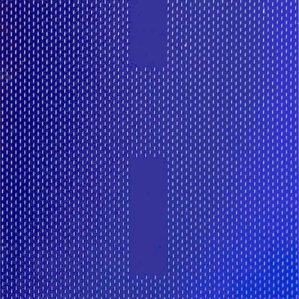
A loophole from the described restrictions of the line opening and the dot opening designs is given by the so-called dash pattern. Such a dashed line pattern consists of scattered lines with an asymmetric relation of the length of the dash and the gap in between two dashes. The ratio between dash and gap is determined by the aluminum paste and the firing conditions used, and allows for a wide range of parameter combinations.
Consequently, the complexity of finding the optimized dash pattern is higher than for a line or dot pattern, but is rewarded by an excellent PERC solar cell performance. The contact formation behavior is comparable to a line pattern and an opening ratio of 1.4% 3% is achieved, which is close to a dot pattern. Additionally, if the rear side bus bar pads, which do not contribute to the electrical contact and BSF formation, are kept free from the LCO process the opening ratio can be optimized further.
Considering the various factors contributing to the performance of the rear side of PERC solar cells, it becomes obvious that the future direction of optimization will be to manage the increasing complexity of the dash pattern design, leading to a layout with changing dash and gap lengths across the wafer. This is related to connected upstream and downstream processes in the production line and will become necessary to achieve the optimum current yield for the solar cell rear side.
Although the performance of PERC solar cells today is often limited by their front side design, it is clear that only with this complexity of the rear contact design, PERC solar cells will reach their efficiency optimum in the future.
There are not only a few technologists, who believe that optimization of the PERC solar cell rear side comes along with a revival of the LDSE technology or the implementation of new metallization schemes such as PoSi in order to overcome the actual limitations of the front side.
In the second part of this article we will cover the next phase of development trends in laser processing for the PV industry.
The second part to the guest blog can viewed here.
Dr. Rico Böhme and Ernst Hartmannsgruber represent laser tool systems manufacturer InnoLas Solutions GmbH.
PV Tech and Solar Intelligence plan to present the most comprehensive and in-depth analysis of the latest manufacturing capacity expansion developments at the inaugural PV CellTech technical conference being held in Kuala Lumpur, Malaysia between 16 – 17 March, 2016. More details on how to attend can be viewed here.


")

