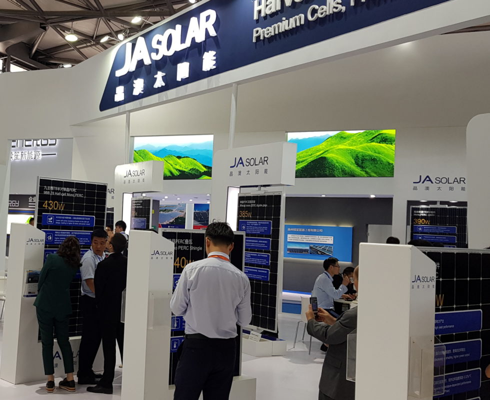
‘Solar Module Super League’ (SMSL) member, JA Solar has licensed a number of patents from Shin-Etsu Chemical on doping Ga in silicon crystals and using the Ga-doped p-type crystalline silicon wafers for making solar cells to mitigate the impact of Light Induced Degradation (LID).
JA Solar indicated that adopting Ga-doped wafer processes would both improve solar cell conversion efficiencies and LID mitigation for advanced solar cells in the future, providing more stable and better long-term energy generation.
Try Premium for just $1
- Full premium access for the first month at only $1
- Converts to an annual rate after 30 days unless cancelled
- Cancel anytime during the trial period
Premium Benefits
- Expert industry analysis and interviews
- Digital access to PV Tech Power journal
- Exclusive event discounts
Or get the full Premium subscription right away
Or continue reading this article for free
Jin Baofang, JA Solar's Chairman of Board of Directors, commented that “using Ga-doped silicon wafers for solar cell application definitely results in better performance of solar cells and PV modules, as well as the improvement of their long-term reliability. Being the patent holder of several leading technologies including bifacial PERC technology in China and other countries, JA Solar has benefited from and always supports IP protection. We deeply appreciate Shin-Etsu Chemical granting JA Solar their IP rights of Ga-doped crystalline silicon technology, which is an important step for JA Solar in introducing advanced technology and supporting the industry's intellectual property protection. JA Solar will continue to develop and provide high-performance PV products and clean-energy solutions to our customers worldwide through technological innovation and continuous performance improvement.”
Typically, monocrystalline solar cells are fabricated on boron doped p-Type wafers but oxygen content can create defects that result in bulk lifetime degradation when the cells are first exposed to light.
There are several possible considerations in using Ga in the crystal growth phase and the need to use consistently high-purity polysilicon in the process. However, the ability to signifcantly reduce LID effects over the lifetime of modules and provide higher overall efficiencies could be the key benefit, especially with next-generation solar cells.

