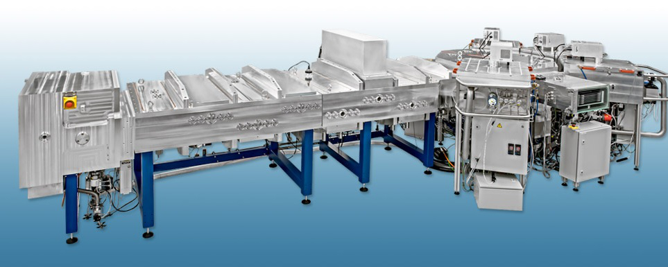
INDEOtec’s Octopus II PECVD system has proven capabilities in the formation of heterojunction solar cells that enables top and bottom side thin film substrate deposition without the need of substrate flipping and vacuum breakage. The proprietary reactor design and a unique electrode arrangement allow low plasma ignition levels and low ion bombardments, which result in superior film thickness uniformity and excellent passivation levels.
Problem
Try Premium for just $1
- Full premium access for the first month at only $1
- Converts to an annual rate after 30 days unless cancelled
- Cancel anytime during the trial period
Premium Benefits
- Expert industry analysis and interviews
- Digital access to PV Tech Power journal
- Exclusive event discounts
Or get the full Premium subscription right away
Or continue reading this article for free
The ability to provide double-sided PECVD deposition of intrinsic and p/n doped a-Si:H layers for heterojunction PV cell devices has the potential to both lower processing costs and provide superior film thickness uniformity and passivation levels that provide higher overall cell conversion efficiencies.
Solution
The OCTOPUS II system generation deploys several new PECVD reactor elements for RF and VHF plasma deposition such as the Mirror reactor concept, which enables the top and bottom side thin film substrate deposition without the need of substrate flipping and vacuum breakage. The proprietary reactor design and a unique electrode arrangement allow low plasma ignition levels and low ion bombardments, which result in superior film thickness uniformity and excellent passivation levels. Another benefit is the capability of creating various, chemically homogeneous thickness profiles across the substrate surface.
Applications
The system can deposit semi-conducting layers: a-Si:H, µc-Si:H, nc-Si:H, SiGe:H etc. Multiple layers (layer stacks) may also be deposited in one reactor without any interruption of the vacuum.
Platform
The OCTOPUS platform the company offers a modular and fully automated cluster deposition system for the deposition of various singular or multiple stacks of thin films by means of PECVD or PVD. The OCTOPUS system significantly reduces the substrate handling and avoids vacuum breakage between top and bottom side deposition cycles.
Availability
Currently available.

")


